Display substrate and display device

A technology for displaying substrates and display areas, which is applied in the direction of identification devices, instruments, etc., and can solve problems such as the influence of color mixing ratio, poor display effect of display devices, and color shift at the junction, so as to achieve uniform color mixing, improve display effect, and reduce color shift The effect of the phenomenon

Active Publication Date: 2015-12-02
BOE TECH GRP CO LTD +1
View PDF7 Cites 31 Cited by
  • Summary
  • Abstract
  • Description
  • Claims
  • Application Information

AI Technical Summary

Problems solved by technology

However, the inventors of the present application found that in this arrangement, the areas of the three sub-pixels covered by the light-shielding layer 2 in the same pixel corresponding to the above-mentioned junction are differ

Method used


Image

  • Display substrate and display device
  • Display substrate and display device
  • Display substrate and display device

Examples


Embodiment approach 1

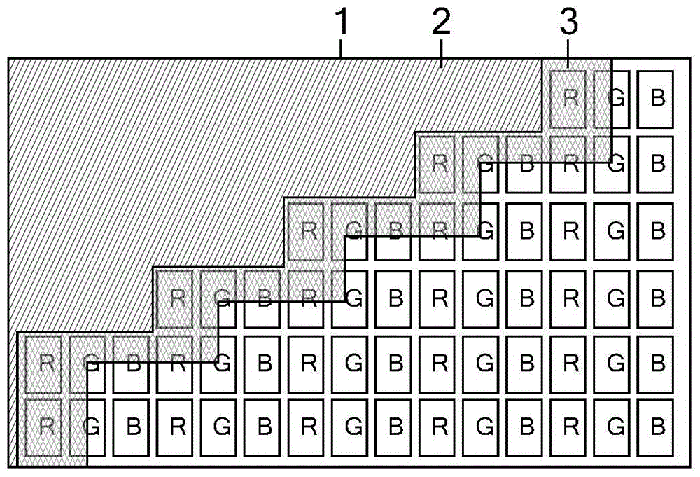
[0035] Embodiment 1, the content of the light-absorbing material in the semi-transparent layer 3 is smaller than the content of the light-absorbing material in the light-shielding layer 2 , and the thickness of the semi-light-transmitting layer 3 is the same as that of the light-shielding layer 2 . In the case of the same thickness, the smaller the content of the light-absorbing material, the weaker the ability to absorb light. Therefore, the ability of the semi-transparent layer 3 to absorb light is weaker than that of the light-shielding layer 2, so that the semi-transparent layer 3 It can allow part of the light incident on it to pass through, so as to achieve the effect of partial light transmission. Further, since the ability of the semi-transparent layer 3 to absorb light is positively correlated with the content of the light-absorbing material, that is, the higher the content of the light-absorbing material in the semi-transparent layer 3, the stronger the ability of the...

Embodiment approach 2

[0036] Embodiment 2, such as Figure 8 As shown, the content of the light-absorbing material in the semi-transparent layer 3 is the same as that in the light-shielding layer 2 , and the thickness of the semi-transparent layer 3 is smaller than that of the light-shielding layer 2 . In the case of the same content of the light-absorbing material, the thickness of the semi-transparent layer 3 is smaller than the thickness of the light-shielding layer 2, so that the propagation distance of the light in the semi-transparent layer 3 is shorter than the propagation distance of the light in the light-shielding layer 2, and then The light-absorbing ability of the semi-transparent layer 3 is weaker than that of the light-shielding layer 2, so that the semi-transparent layer 3 allows part of the light incident thereto to pass through. Further, since the thickness of the semi-transparent layer 3 is larger, the longer the propagation distance of the light in the semi-transparent layer 3, t...


PUM


Abstract

The invention discloses a display substrate and a display device and relates to the technical field of display. The display substrate and the display device are used for improving the display effect of the display device. The display substrate comprises a display area and a non-display area shielded by a shading layer. A semi-light-transmitting layer is arranged on the intersection of the non-display area and the display area. Brightness contrast of the intersection of the display area and the non-display area is weakened through the semi-light-transmitting layer, so that the sawtooth-shaped intersection is fuzzy, part of light emitted by three sub-pixels in the same pixel corresponding to the intersection is allowed to pass, and accordingly the color error phenomenon of the intersection is weakened. The display substrate and the display device are used for forming a non-rectangular display area on the display substrate.

Description

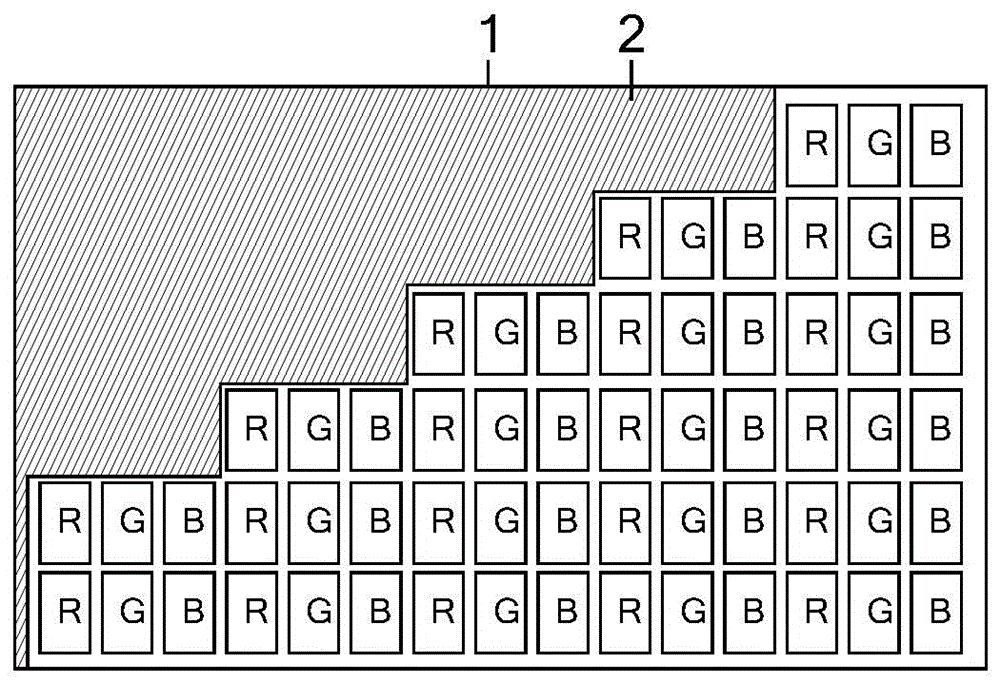
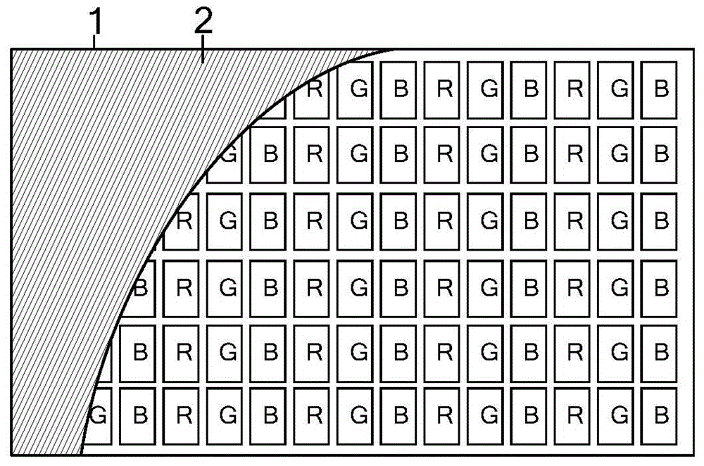
technical field [0001] The present invention relates to the field of display technology, in particular to a display substrate and a display device. Background technique [0002] At present, in order to meet the needs of users for personalized customization, the display area in the display substrate is often designed to be non-rectangular. For example, if figure 1 and figure 2 As shown, the pixels on the display substrate 1 are still arranged in the form of a two-dimensional matrix, and the two-dimensional matrix includes a plurality of pixel rows and pixel columns, wherein each pixel includes three sub-pixels, and the three sub-pixels are respectively used to display red, For green and blue, by setting the light-shielding layer 2 on the display substrate 1, the pixels in the non-display area are properly shielded to form a non-rectangular display area. Specifically, there are two main ways to set up the light-shielding layer 2: [0003] Setting method one, such as figu...

Claims


Application Information

Patent Timeline
IPC IPC(8): G09F9/00
Inventor 韦东梅祁小敬邓银李坤
Owner BOE TECH GRP CO LTD
Why Eureka
Try Eureka