Etching method

An etching gas, etching rate technology, applied in electrical components, semiconductor/solid-state device manufacturing, circuits, etc., can solve the difficult pattern of photoresist, pattern deformation, and photoresist cannot provide sufficient etching resistance and other problems to achieve the effect of avoiding inaccurate patterns and reducing the degree of etching

Active Publication Date: 2018-06-29
SEMICON MFG INT (SHANGHAI) CORP
View PDF4 Cites 0 Cited by
  • Summary
  • Abstract
  • Description
  • Claims
  • Application Information

AI Technical Summary

Problems solved by technology

[0004] However, reducing the thickness of the photoresist can easily lead to the fact that the thinner photoresist cannot provide sufficient etching resistance. When the photoresist is used as an etching mask to transfer the pattern in the photoresist to the etched material layer During the process, it may be difficult for the photoresist to play a good role in blocking the etching, that is to say, after the etching is carried out to a certain extent, the photoresist will be too thin to accurately define the etched area below. The pattern of the etched material layer, which leads to the relative deformation of the pattern morphology formed in the etched material layer

Method used


Image

  • Etching method
  • Etching method
  • Etching method

Examples


Embodiment Construction

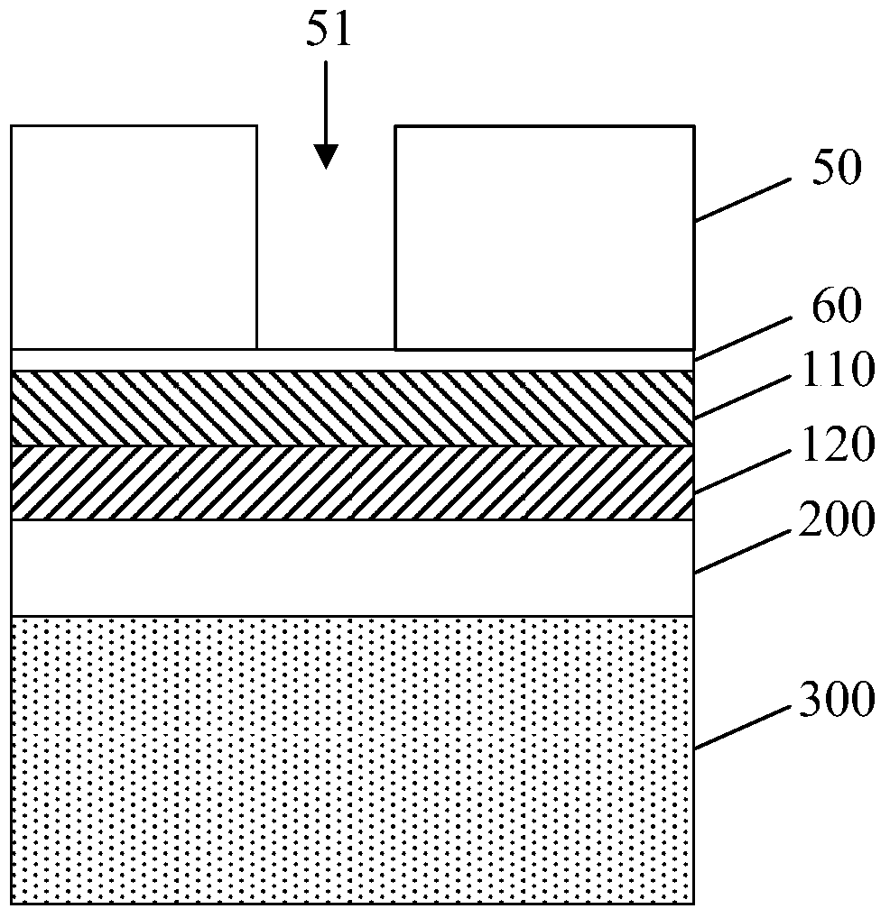
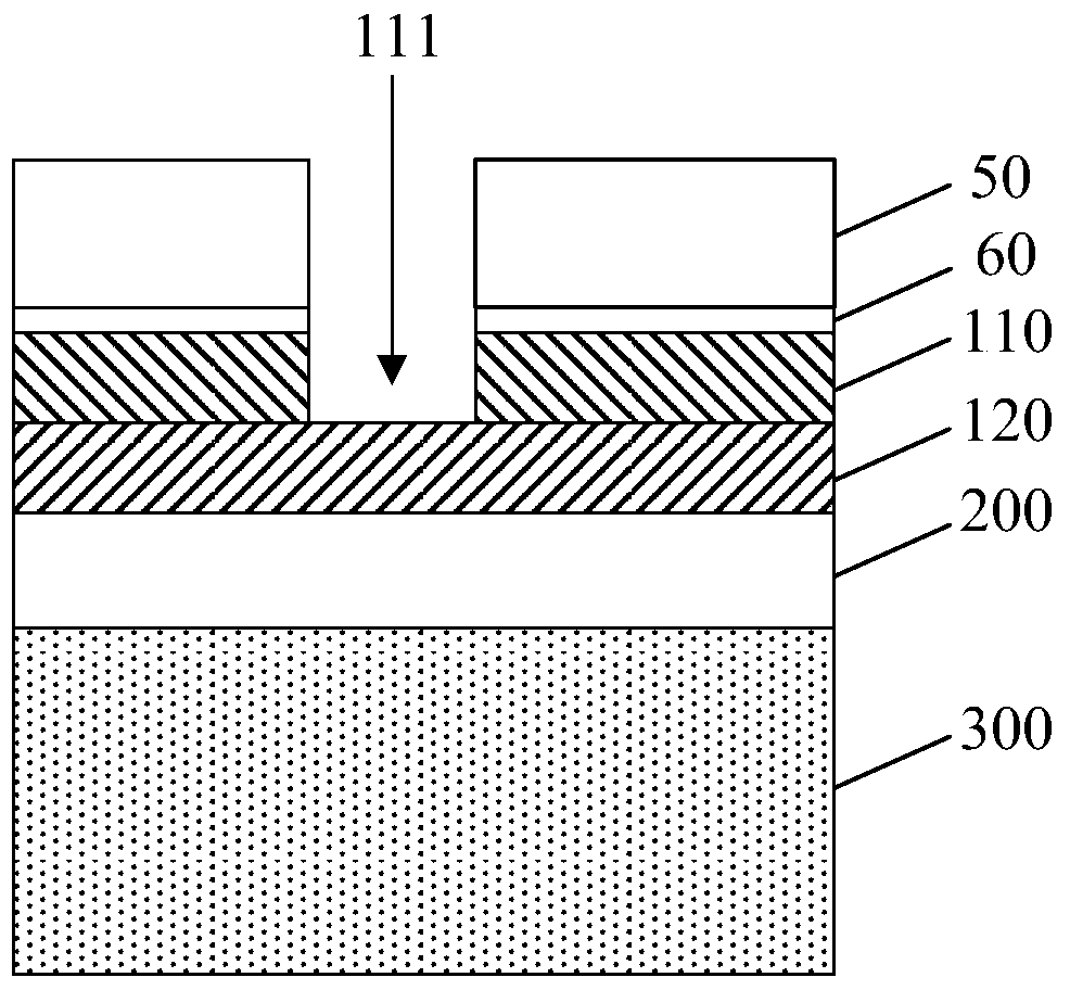
[0044] In the prior art, in order to better transfer the pattern in the photoresist to the material layer to be etched, a layer of hard mask (hard mask) is added between the photoresist and the material layer to be etched. For the hard mask, the pattern in the photoresist is first transferred to the hard mask, and then the remaining hard mask is used as an etching mask to transfer the pattern to the etched material layer.

[0045] However, since the prior art needs to form a thinner photoresist (ultra thin PR), it cannot block the etching well, resulting in deformation of the pattern transferred into the hard mask, so that the pattern cannot be transferred well. Into the etched material layer, which in turn affects the topography of the pattern formed by etching.

[0046] Therefore, the present invention provides an etching method, comprising: providing a substrate; forming an etching material layer on the substrate; forming a hard mask on the etching material layer, and the h...


PUM


Abstract

The invention provides an etching method. The method comprises providing a substrate, forming an etching material layer on the substrate, forming hard masks, which comprises a second hard mask and a first hard mask successively formed on the etching material layer, on the etching material layer, enabling the first hard mask to be graphical, forming a pattern in the first hard mask, enabling part of the second hard mask to be exposed, etching the second hard mask taking the first hard mask as a mask, transferring the pattern onto the second hard mask, and etching the material layer taking the second hard mask, having the pattern, as the mask. The etching method is advantageous in that, compared with a mode that hard masks are etched completely by utilizing first photoresist in the prior art, the etching method reduces the etched degree of the first photoresist, and then the problem that the patterns formed in the hard masks are not precise enough due to the too thin first photoresist is prevented as far as possible.

Description

technical field [0001] The invention relates to the field of semiconductor manufacturing, in particular to an etching method. Background technique [0002] The feature size of semiconductor devices is gradually decreasing, which puts more requirements on the manufacturing process of semiconductor devices. [0003] For example, in order to reduce the size of the semiconductor device as much as possible, it is required that the size and thickness of each component or material layer in the semiconductor device become smaller. Among them, the thickness of the photoresist coated in the photolithography process is also required to be reduced, thereby providing conditions for manufacturing semiconductor devices with smaller feature sizes. [0004] However, reducing the thickness of the photoresist can easily lead to the fact that the thinner photoresist cannot provide sufficient etching resistance. When the photoresist is used as an etching mask to transfer the pattern in the phot...

Claims


Application Information

Patent Timeline
Patent Type & Authority Patents(China)
IPC IPC(8): H01L21/311H01L21/027H01L21/033
Inventor 张海洋周俊卿
Owner SEMICON MFG INT (SHANGHAI) CORP
Why Eureka
Try Eureka