Sensing circuit and corresponding OLED display equipment

一种感测电路、显示设备的技术,应用在电路、电气元件、电固体器件等方向,能够解决薄膜晶体管开启电压偏移、显示画质不均匀等问题

Active Publication Date: 2016-01-27
TCL CHINA STAR OPTOELECTRONICS TECH CO LTD
View PDF4 Cites 42 Cited by
  • Summary
  • Abstract
  • Description
  • Claims
  • Application Information

AI Technical Summary

Problems solved by technology

[0005] Due to the aging of thin film transistors and OLED panels, the turn-on voltage of thin film transistors is shifted by Vth_TFT, and the shift of Vth_oled occurs in OLEDs, resulting in uneven display quality.

Method used


Image

  • Sensing circuit and corresponding OLED display equipment
  • Sensing circuit and corresponding OLED display equipment
  • Sensing circuit and corresponding OLED display equipment

Examples


Embodiment Construction

[0023] The following descriptions of the various embodiments refer to the accompanying drawings to illustrate specific embodiments in which the present invention can be practiced.

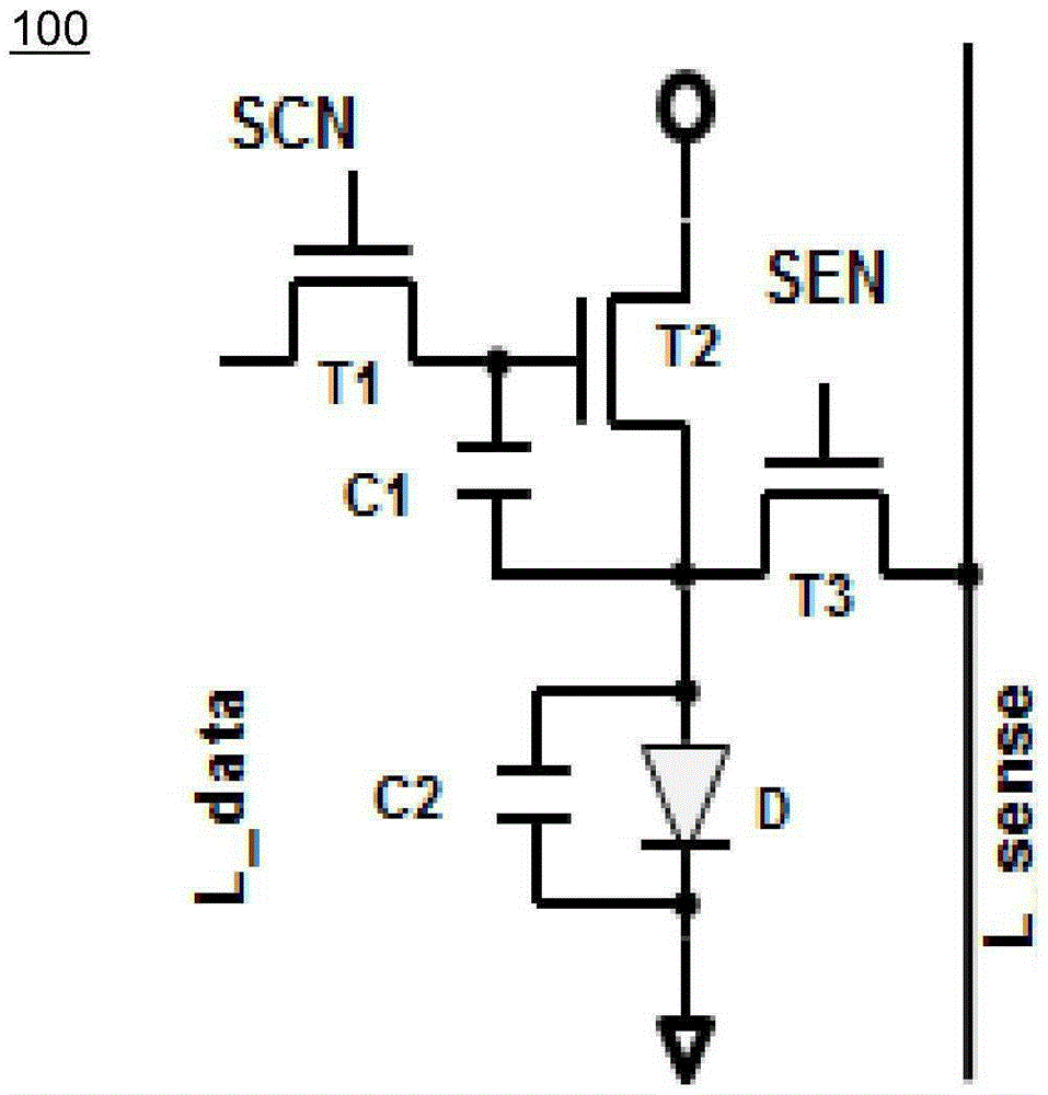
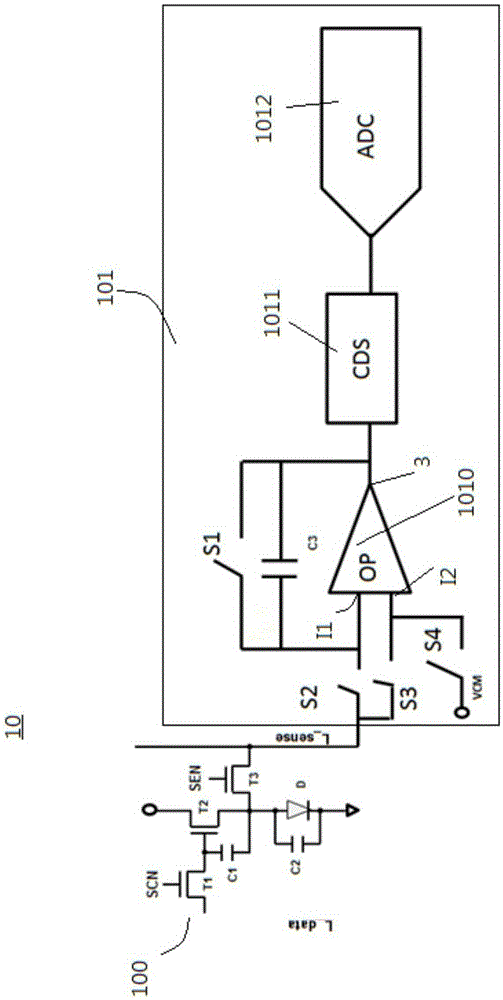
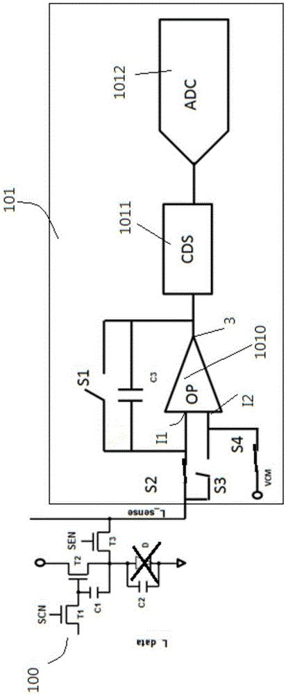
[0024] refer to image 3 , image 3 is a schematic diagram of a sensing circuit 10 according to an embodiment of the present invention. The sensing circuit 10 includes a pixel circuit 100, and the pixel circuit 100 includes: a data line L_data for inputting data; a first thin film transistor T1; a second thin film transistor T2, the second thin film transistor T2 A gate of the first thin film transistor is connected to the drain of the first thin film transistor; a third thin film transistor T3, a source of the third thin film transistor T3 is connected to a drain of the second thin film transistor; a second thin film transistor T3 Capacitor C1, connected to the gate and a drain of the second thin film transistor T2; an organic light emitting diode D, connected to the drain of the second thin fil...


PUM


Abstract

The invention brings forward a sensing circuit to sense micro currents and voltages of a device to be sensed. OLED display equipment comprises: a pixel circuit and the sensing circuit. The sensing circuit is connected to the pixel circuit through sensing lines. The sensing circuit comprises: an amplifier, a first capacitor, a first switch, a second switch, a third switch, a fourth switch, a correlated double sampling (CDS) circuit, and an analog-digital converter (ADC).

Description

【Technical field】 [0001] The invention relates to a sensing circuit, which is used for sensing the tiny current and voltage of a device to be sensed, especially a sensing circuit suitable for an organic light-emitting diode (Organic Light-Emitting Diode, OLED) display. 【Background technique】 [0002] OLED display technology is different from the traditional LCD display method. OLED does not use a backlight, but uses a very thin organic material coating and a glass substrate, and the current passes through it to make the organic material emit light. OLED display screens are usually thinner and lighter, have a larger viewing angle, and save more power. [0003] figure 1 It is a schematic diagram of a pixel circuit of an existing OLED panel, the pixel circuit includes a data line for inputting data; a first thin film transistor and a second thin film transistor, a gate of the second thin film transistor is connected to the A drain of the first thin film transistor; a second c...

Claims


Application Information

Patent Timeline
Patent Type & Authority Applications(China)
IPC IPC(8): G09G3/3233
CPCG09G2320/0233G09G2320/045G09G2330/12G09G3/3233H10K59/131G09G3/3258H01L27/124
Inventor 黄泰钧梁鹏飞
Owner TCL CHINA STAR OPTOELECTRONICS TECH CO LTD
Why Eureka
Try Eureka