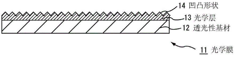
Optical film and display device with contact control plate
A touch panel, optical film technology, applied in optics, optical components, instruments, etc., can solve problems such as inability to fully suppress glare
- Summary
- Abstract
- Description
- Claims
- Application Information
AI Technical Summary
Problems solved by technology
Method used
Image

Examples
Embodiment 1
[0339] (production of optical film)
[0340] Prepare a light-transmitting substrate (cellulose triacetate film, thickness 40 μm, manufactured by Konica Minolta, KC4UAW), and coat the optical layer composition of the following composition on one side of the light-transmitting substrate, Form a coating film.
[0341] Next, for the formed coating film, dry air at 50° C. was circulated at a flow rate of 0.2 m / s for 30 seconds, and then dried at a flow rate of 10 m / s at 70° C. for 30 seconds. Thereby, the solvent in the coating film is evaporated.
[0342] Then, using an ultraviolet irradiation device (manufactured by FusionUV Systems Japan, light source H bulb), under a nitrogen atmosphere (oxygen concentration 200ppm or less), the cumulative light intensity is 100mJ / cm 2 The coating film was cured by irradiating ultraviolet rays in such a manner that an optical layer having a thickness of 5.0 μm (at the time of curing) was formed to produce an optical film.
[0343] (compositi...
Embodiment 2
[0346] In addition to making the curing conditions of the coating film such that the cumulative light intensity of ultraviolet rays is 50mJ / cm 2 The concave-convex layer was formed in the same manner as the optical layer of Example 1, except that the coating film was cured by irradiation in the same manner.
[0347] The composition for the low-refractive-index layer shown below was coated on the surface of the formed uneven|corrugated layer, and the coating film was formed.
[0348] Next, for the formed coating film, dry air at 40° C. was circulated at a flow rate of 0.2 m / s for 15 seconds, and then dried at a flow rate of 10 m / s at 40° C. for 30 seconds. This evaporates the solvent in the coating film.
[0349] Then, using an ultraviolet irradiation device (manufactured by FusionUV Systems Japan, light source H bulb), under a nitrogen atmosphere (oxygen concentration 200ppm or less), the cumulative light intensity is 100mJ / cm 2 The coating film was cured by irradiating ultr...
Embodiment 3
[0354] In addition to making the mixing amount of silica fine particles in the composition for optical layers 0.8 parts by mass, the drying conditions of the coating film were to circulate dry air at 70° C. An optical film was produced in the same manner as in Example 1 except that 70° C. dry air was circulated at a flow rate of s for 30 seconds.
PUM
| Property | Measurement | Unit |
|---|---|---|
| Average primary particle size | aaaaa | aaaaa |
| Thickness | aaaaa | aaaaa |
| The average particle size | aaaaa | aaaaa |
Abstract
Description
Claims
Application Information
 - R&D Engineer
- R&D Manager
- IP Professional
- Industry Leading Data Capabilities
- Powerful AI technology
- Patent DNA Extraction
Browse by: Latest US Patents, China's latest patents, Technical Efficacy Thesaurus, Application Domain, Technology Topic.
© 2024 PatSnap. All rights reserved.Legal|Privacy policy|Modern Slavery Act Transparency Statement|Sitemap