Photoresistor and manufacturing method thereof

A technology of photoresistor and manufacturing method, applied in circuits, electrical components, semiconductor devices, etc., can solve the problems of high rejection rate, reduced performance parameters of photoresistors, poor stability, etc., and achieves reduction in rejection rate, increased dark resistance, stability high effect

Active Publication Date: 2016-02-17
NANYANG NORMAL UNIV
View PDF4 Cites 11 Cited by
  • Summary
  • Abstract
  • Description
  • Claims
  • Application Information

AI Technical Summary

Problems solved by technology

Although adding CuCl 2 The material method can improve the sensitivity of photoresistors, but due to the instability of copper ions, that is, monovalent copper ions and divalent copper ions will change each other, which will cause the performance parameters of photoresistors to decrease after the aging process, and the stability is relatively low. Poor, one of the outstanding performances is the high scrap rate, reaching about 15%

Method used


Image

  • Photoresistor and manufacturing method thereof
  • Photoresistor and manufacturing method thereof
  • Photoresistor and manufacturing method thereof

Examples


Embodiment 1

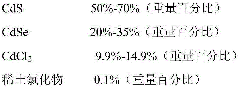
[0035] Embodiment 1: A kind of photoresistor, comprises ceramic substrate, photosensitive layer and two electrodes, photosensitive layer is coated on the surface of ceramic substrate, photosensitive layer and ceramic substrate form photoresistor main body, two electrodes are installed on two sides of photoresistor main body respectively At the end, the photosensitive layer consists of the following components:

[0036]

[0037]

[0038] The rare earth chloride is one of holmium chloride, neodymium chloride, gadolinium chloride, dysprosium chloride and samarium chloride or a mixture of two or more.

Embodiment 2

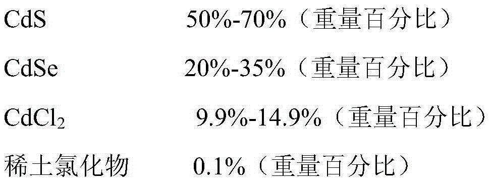
[0039] Embodiment 2: A kind of photoresistor, comprises ceramic substrate, photosensitive layer and two electrodes, photosensitive layer is coated on the surface of ceramic substrate, photosensitive layer and ceramic substrate form photoresistor main body, two electrodes are respectively installed on two sides of photoresistor main body At the end, the photosensitive layer consists of the following components:

[0040]

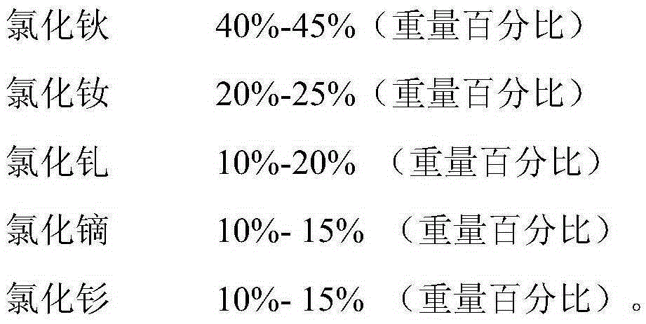
[0041] In this embodiment, the rare earth chloride is a mixture of holmium chloride, neodymium chloride, gadolinium chloride, dysprosium chloride and samarium chloride, and the rare earth chloride is composed of the following components:

[0042]

[0043] In this embodiment, the thickness of the photosensitive layer is 5 microns.

[0044] In this embodiment, the ceramic substrate is prepared from Al2O3 with a purity of more than 93%.

Embodiment 3

[0045]Embodiment 3: A kind of photoresistor, comprises ceramic substrate, photosensitive layer and two electrodes, photosensitive layer is coated on the surface of ceramic substrate, photosensitive layer and ceramic substrate form photoresistor main body, two electrodes are respectively installed on two sides of photoresistor main body At the end, the photosensitive layer consists of the following components:

[0046]

[0047] In this embodiment, the rare earth chloride is a mixture of holmium chloride, neodymium chloride, gadolinium chloride, dysprosium chloride and samarium chloride, and the rare earth chloride is composed of the following components:

[0048]

[0049]

[0050] In this embodiment, the thickness of the photosensitive layer is 2 microns.

[0051] In this embodiment, the ceramic matrix is ​​prepared from Al2O3 with a purity of more than 93%.


PUM

PropertyMeasurementUnit
Thicknessaaaaaaaaaa
Thicknessaaaaaaaaaa
Thicknessaaaaaaaaaa

Abstract

The invention discloses a photoresistor and a manufacturing method thereof. The method is characterized by adopting rare-earth chloride to replace CuCl; adding the rare-earth chloride, the weight percentage of which is 0.1%, to photosensitive layer materials CdS, CdSe and CdCl2, wherein the rare-earth chloride is one or a mixture of two or more than two of holmium chloride, neodymium chloride, gadolinium chloride, dysprosium chloride and samarium chloride; and adjusting proportion of the three materials of CdS, CdSe and CdCl2, wherein the rare-earth chloride content is very small, so that the material cost of the photoresistor is not influenced, and through the combination of the rare-earth chloride and the three materials of CdS, CdSe and CdCl2, dark resistance of the photoresistor can be increased, and bright resistance of the photoresistor can be can be reduced. The advantages are that sensitivity of the photoresistor can be improved; the stability of the rare-earth chloride is relatively high, so that the photoresistor is not easy to change in the aging process, and reduction of other performance parameters of the photoresistor does not be caused; and since the stability of the photoresistor in the in the aging process is high, rejection rate is greatly reduced.

Description

technical field [0001] The invention relates to a photosensitive resistor, in particular to a photosensitive resistor and a manufacturing method thereof. Background technique [0002] Photoresistors are mainly used in various photoelectric control systems, such as photoelectric automatic switch portals, automatic lighting systems, automatic water supply devices, mechanical automatic protection devices, photoelectric counters, and photoelectric tracking systems. [0003] Existing photoresistors generally include a ceramic substrate, a photosensitive layer and two electrodes. The photosensitive layer is coated on the surface of the ceramic substrate. The photosensitive layer and the ceramic substrate form the main body of the photoresistor. The two electrodes are respectively installed at both ends of the main body of the photoresistor. The resistance value of the photoresistor measured after a certain period of time after it is completely dark at room temperature is called da...

Claims


Application Information

Patent Timeline
IPC IPC(8): H01L31/0296H01L31/08
CPCH01L31/0296H01L31/085
Inventor 鲁道邦朱永胜宋玉玲惠明海涛孙国良
Owner NANYANG NORMAL UNIV
Why Eureka
Try Eureka