Pixel array and repairing method for pixel unit

A pixel array and pixel unit technology, applied in electrical components, optics, instruments, etc., can solve the problems of pixel electrodes not being connected to the common potential, failure of dark spots, complex display panels, etc., and achieve good display quality.

Inactive Publication Date: 2016-03-23
AU OPTRONICS CORP
View PDF5 Cites 9 Cited by
  • Summary
  • Abstract
  • Description
  • Claims
  • Application Information

AI Technical Summary

Problems solved by technology

However, since the structure of the display panel tends to be complex, the pixel electrodes may still not be connected to the common potential after repairing, resulting in the failure of dark spots

Method used


Image

  • Pixel array and repairing method for pixel unit
  • Pixel array and repairing method for pixel unit
  • Pixel array and repairing method for pixel unit

Examples


Embodiment Construction

[0067] Below in conjunction with accompanying drawing, structural principle and working principle of the present invention are described in detail

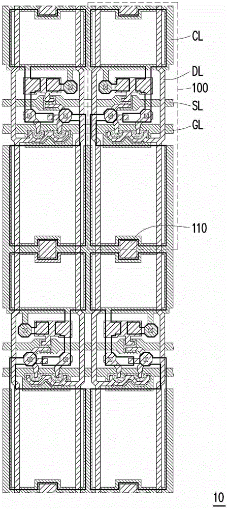
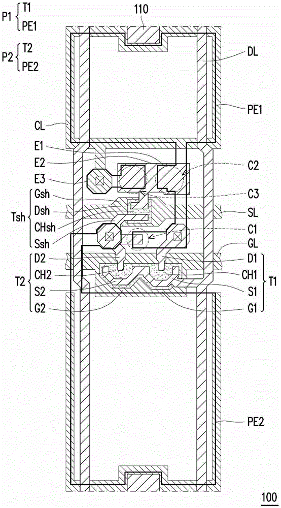
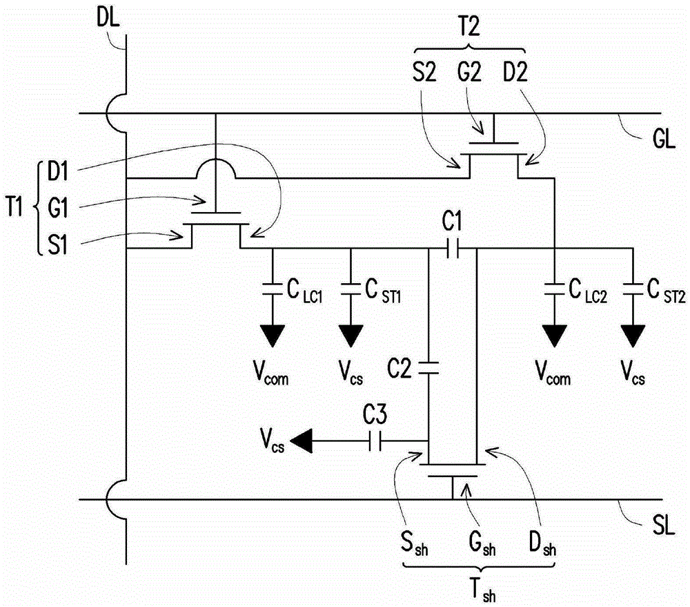
[0068] Figure 1A is a schematic diagram of a pixel array according to an embodiment of the present invention, Figure 1B for Figure 1A A partial enlarged schematic diagram of a pixel unit, Figure 1C for Figure 1B Schematic diagram of the equivalent circuit of the pixel unit. For the convenience of illustration, in Figure 1AIn the figure, it is taken that the pixel array includes 2×2 pixel units as an example, but the present invention is not limited thereto.

[0069] Please also refer to Figure 1A to Figure 1C , the pixel array 10 includes a plurality of pixel units 100 . Each pixel unit 100 includes a first sub-pixel P1, a second sub-pixel P2, a scan line GL and a data line DL. The first sub-pixel P1 includes a first active element T1 and a first pixel electrode PE1. The first active device T1 includes, for example, a...


PUM


Abstract

The invention provides a pixel array and a repairing method for a pixel unit. The pixel array comprises a plurality of pixel units. Each pixel unit comprises a first sub-pixel and a second sub-pixel. The first sub-pixel comprises a first active element and a first pixel electrode electrically connected to the drain electrode of the first active element. The second sub-pixel comprises a second active element and a second pixel electrode electrically connected to the drain electrode of the second active element. The overlapped part of the first pixel electrode and the drain electrode of the second active element is provided with a first capacitor. The present invention also provides a repairing method for a pixel unit.

Description

technical field [0001] The invention relates to a pixel array and a pixel unit repairing method, in particular to a pixel array and a pixel unit repairing method which are beneficial to dark spots. Background technique [0002] In recent years, although flat panel display technology has matured, some dot defects will inevitably occur in the manufacturing process of the components of the display panel, such as the active device array substrate. Generally speaking, if the aforementioned dot defects can be repaired into dark dots by means of repairing, these defective display panels can be discarded without scrapping. [0003] The current repairing method of pixel unit usually adopts laser welding (laser welding) and laser cutting (laser cutting) to carry out, so as to connect the pixel electrode to the common potential, and then achieve the dark spot effect. However, since the structure of the display panel tends to be complicated, the pixel electrodes may still not be reliab...

Claims


Application Information

Patent Timeline
IPC IPC(8): G02F1/13H01L27/12
CPCG02F1/1309H01L27/1255
Inventor 林禹佐林庭谊简伯儒吴贞仪
Owner AU OPTRONICS CORP
Why Eureka
Try Eureka