Supercharge Your Innovation With Domain-Expert AI Agents!

Wafer transmission device and vacuum adsorption manipulator thereof

A vacuum adsorption and manipulator technology, which is applied to conveyor objects, transportation and packaging, electrical components, etc., can solve the problems of unqualified wafer 1, reduce the qualified rate of wafer 1, etc., and achieve the effect of improving the qualified rate

Active Publication Date: 2016-03-23
SHANGHAI HUAHONG GRACE SEMICON MFG CORP
View PDF4 Cites 3 Cited by
  • Summary
  • Abstract
  • Description
  • Claims
  • Application Information

AI Technical Summary

Problems solved by technology

[0005] However, it is found in the course of use that after the wafer is transported to the desired position using the above-mentioned vacuum adsorption manipulator, if image 3 As shown, there is a mark 6 formed on the back of the wafer 1 in contact with the vacuum suction manipulator, causing the wafer 1 with the mark 6 to be unqualified and reducing the pass rate of the wafer 1

Method used


Image

  • Wafer transmission device and vacuum adsorption manipulator thereof
  • Wafer transmission device and vacuum adsorption manipulator thereof
  • Wafer transmission device and vacuum adsorption manipulator thereof

Examples


no. 1 example

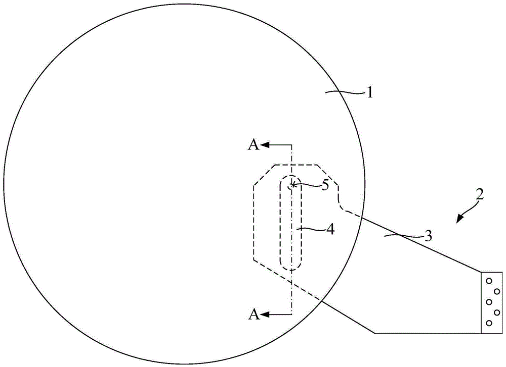
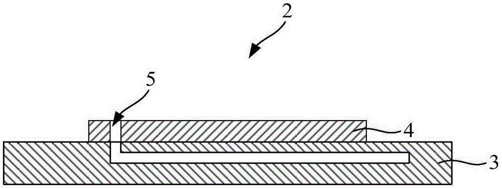
[0039] combine Figure 4 to Figure 5 As shown, this embodiment provides a vacuum suction manipulator 10 for transferring wafers, which includes an arm 11 , and a suction insulating boss 12 and a dummy insulating boss 13 fixed on the arm 11 . Wherein, the adsorption insulating boss 12 is ring-shaped, and the false insulating boss 13 is located in the adsorption insulating boss 12, and is integrally formed with the arm 11. On the direction V perpendicular to the arm 11, the adsorption insulating boss 12 is larger than the pseudo insulating boss 12 13 stand out.

[0040] The arm 11, the false insulation boss 13 and the adsorption insulation boss 12 are provided with a vacuum air channel 14, and according to the flow direction of the air in the vacuum air channel 14, the vacuum air channel 14 is successively formed by the first segment air channel 140 (in the figure). Shown by dotted lines), the second segment air channel 141, and the third segment air channel 142, wherein the fi...

no. 2 example

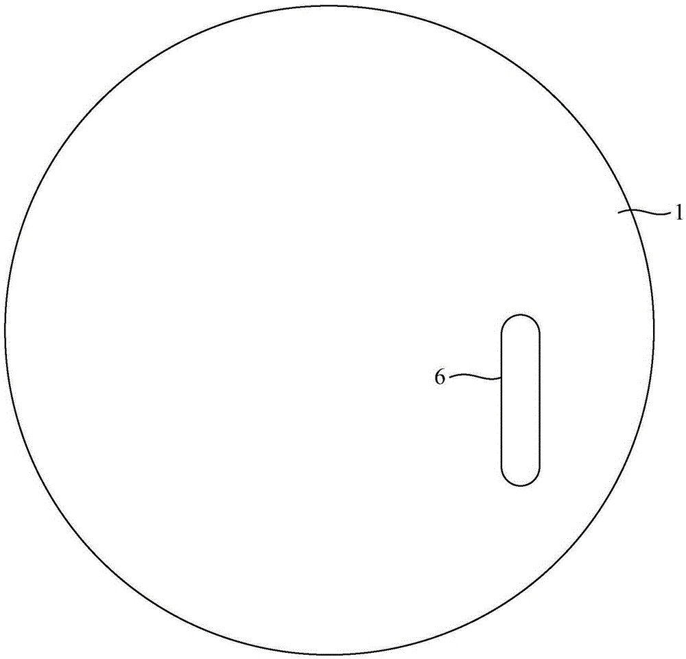
[0050] combine Figure 6 to Figure 7 As shown, the difference between the second embodiment and the first embodiment is that in the second embodiment, no pseudo-adsorption boss is set in the vacuum adsorption manipulator 10, and the adsorption insulation boss 12 is a solid column, and the vacuum air channel 14 is arranged on the arm 11 and the adsorption insulation boss 12.

[0051] It should be noted that, in the technical solution of the present invention, the adsorption insulating bosses, arms, and false insulating bosses can be set in any shape, and should not be limited to those shown in the accompanying drawings.

[0052] In addition, the present invention also provides a wafer transfer device, which includes the above-mentioned vacuum adsorption manipulator.


PUM


Abstract

The invention provides a wafer transmission device and a vacuum adsorption manipulator thereof. The vacuum adsorption manipulator comprises an arm, an insulative adsorption boss fixed on the arm, and a vacuum air passage formed in the arm and the insulative adsorption boss, wherein the insulative adsorption boss is used for adsorbing the back surface of a wafer to be transmitted, and is softer than the back surface of the wafer to be transmitted. As the insulative adsorption boss is softer than the back surface of the wafer to be transmitted, after the vacuum adsorption manipulator transmits the wafer to a required position, no imprint is formed in the position, in contact with the vacuum adsorption manipulator, on the back surface of the wafer, that is, the qualified rate of wafers is improved.

Description

technical field [0001] The invention relates to the technical field of semiconductor manufacturing equipment, in particular to a wafer transfer device and a vacuum adsorption manipulator thereof. Background technique [0002] In many semiconductor processes, it is necessary to use a wafer transfer device to transfer wafers. Existing wafer transfer devices all include a vacuum suction manipulator, which utilizes the principle of vacuum suction to absorb the wafer to transfer the wafer to a desired location. [0003] combine Figure 1 to Figure 2 As shown, the vacuum adsorption manipulator 2 of the existing wafer transfer device includes an arm 3 and an adsorption insulation boss 4 fixed on the arm 3 , and the adsorption insulation boss 4 and the arm 3 are integrally formed. The projected area of ​​the adsorption insulating boss 4 along the direction perpendicular to the arm 3 is smaller than that of the arm 3 , and a vacuum air passage 5 is arranged inside the arm 3 and the ...

Claims


Application Information

Patent Timeline
Patent Type & Authority Applications(China)
IPC IPC(8): H01L21/677H01L21/683
CPCH01L21/677H01L21/6838
Inventor 王磊曹圣豪秦羽
Owner SHANGHAI HUAHONG GRACE SEMICON MFG CORP
Features
  • R&D
  • Intellectual Property
  • Life Sciences
  • Materials
  • Tech Scout
  • Unparalleled Data Quality
  • Higher Quality Content
  • 60% Fewer Hallucinations
Learn More