Display panel and display device

A display panel and edge pixel technology, applied in radiation control devices, static indicators, instruments, etc., can solve the problems of reduced visual effects at the edge of the display panel, affecting user experience, etc., to improve the visual effect of the edge and reduce the "jaggy" vision effect, the effect of improving user experience

Active Publication Date: 2016-04-20
BOE TECH GRP CO LTD +1
View PDF4 Cites 48 Cited by
  • Summary
  • Abstract
  • Description
  • Claims
  • Application Information

AI Technical Summary

Problems solved by technology

[0004] The present invention aims at reducing the visual effect of the edge of the display panel and affecting the user experience caused by the non-smooth boundary line visible on the edge of the existing special-shaped panel, and provides a display that can improve the visual effect of the edge of the display panel and improve the user experience. Panels and Displays

Method used


Image

  • Display panel and display device
  • Display panel and display device
  • Display panel and display device

Examples


Embodiment 1

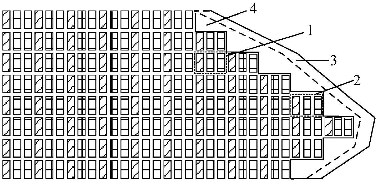
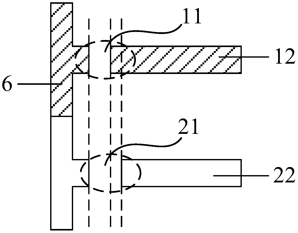
[0026] Please refer to figure 1 and figure 2 , this embodiment provides a display panel, including multiple rows of pixel units, the edges of the multiple rows of pixel units are arranged in steps, each row of pixel units includes a central pixel unit 1 and an edge pixel unit 2, and each central pixel unit 1 includes multiple sub-pixels and a first thin-film transistor corresponding to each sub-pixel, the first thin-film transistor has a first semiconductor region 11; each edge pixel unit 2 includes a plurality of sub-pixels and a second thin-film transistor corresponding to each sub-pixel, the second thin-film transistor The transistor has a second semiconductor region 21; the length of the first semiconductor region 11 is set to a first set length, the width of the first semiconductor region 11 is set to a first set width, and the length of the second semiconductor region 21 is set to a second set length. The width of the second semiconductor region 21 is set to a second s...

Embodiment 2

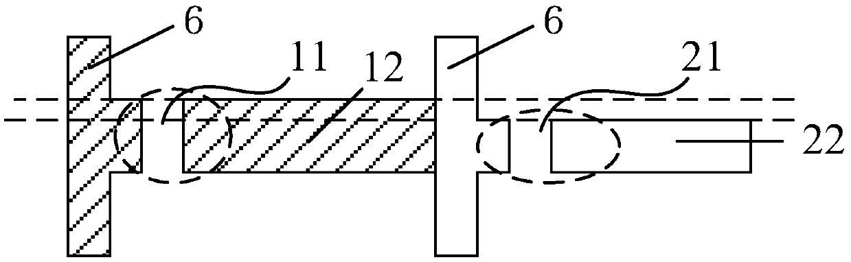
[0036] Please refer to figure 1 and image 3 , this embodiment provides a display panel, which has a structure similar to that of the display panel in Embodiment 1. The difference between it and Embodiment 1 lies in that the second set width is smaller than the first set width.

[0037] It should be noted that the width of the channel region in this embodiment refers to the length through which carriers pass, such as figure 2 As shown, the left side of each pixel unit can be regarded as the pixel electrode signal line 6 for supplying voltage. In fact, the pixel electrode signal line 6 is an integral structure. figure 2 The above is only to distinguish the different parts of the pixel electrode signal line 6 corresponding to different pixel units, so the different parts of the pixel electrode signal line 6 are colored differently, the right side is the pixel electrode, and the part between the pixel electrode signal line 6 and the pixel electrode The region is the channel r...

Embodiment 3

[0041] Please refer to Figure 4 and Figure 5 , this embodiment provides a display panel, which has a structure similar to that of the display panel in Embodiment 1. The difference between it and Embodiment 1 is that each row of pixel units further includes: sub-edge pixel units 5 .

[0042] In this embodiment, the sub-edge pixel unit 5 is located between the central pixel unit 1 and the edge pixel unit 2 . Specifically, the sub-edge pixel unit 5 refers to a pixel unit where one side connects to the filling area 4 .

[0043] Each sub-edge pixel unit 5 includes a plurality of sub-pixels (generally including R sub-pixels, G sub-pixels and B sub-pixels) and a third thin film transistor (not shown) corresponding to each sub-pixel, the third thin film transistor has The third semiconductor region 51, the length of the third semiconductor region 51 is a third set length, and the width of the third semiconductor region 51 is a third set width.

[0044] It should be noted that the...


PUM


Abstract

The invention provides a display panel and a display device, belonging to the display technical field, and solves the problems of the reduced display panel edge visual effect and the influence to user experiences caused by visual uneven border lines of present special-shaped panel edges. In the display panel, the edges of a plurality of rows of pixel units are arranged in a ladder pattern; each row of pixel units comprises a central pixel unit and an edge pixel unit. Each central pixel unit comprises a first film transistor corresponding to each sub-pixel; the first film transistor is provided with a first semiconductor zone; each edge pixel unit comprises a second film transistor corresponding to each sub-pixel; the second film transistor is provided with a second semiconductor zone. The length and width of the first semiconductor zone are set to be a first set length and a first set width, and the length and width of the second semiconductor zone are set to be a second set length and a second set width, thereby allowing the brightness of an edge pixel unit to be less than the brightness of a central pixel unit.

Description

technical field [0001] The invention belongs to the field of display technology, and in particular relates to a display panel and a display device. Background technique [0002] With the development of smart technology, wearable devices are becoming more and more popular, and with the development of wearable electronic products, the human-computer interaction interface of these wearable devices no longer uses traditional rectangular panels, but more and more uses Special-shaped cutting panels, including round, octagonal and even special-shaped cutting corners, to meet the wearable performance of smart devices, or to meet their stylish design. [0003] But there are at least the following problems in the prior art: the special-shaped display panel includes a display area (ie, a pixel area), a black matrix area, and a filling area. Of course, in order to avoid light leakage, the filling area also needs to be filled with black matrix materials. Since the conventional pixel des...

Claims


Application Information

Patent Timeline
Patent Type & Authority Applications(China)
IPC IPC(8): H01L27/146G02F1/133
CPCG02F1/133H01L27/14603G02F2201/56H01L27/1222G02F1/134309G02F1/1368G02F1/13624H01L27/1233G02F1/134345G02F1/015H01L27/1251
Inventor 龙跃王杨刘庭良
Owner BOE TECH GRP CO LTD
Why Eureka
Try Eureka