
Semiconductor Optical Amplifiers for Optical Communication Systems

A technology of optical communication system and optical amplifier, which is applied in the field of optical communication, can solve problems such as rising, unfavorable cost, additional energy consumption, and decreased transmission performance, so as to reduce power damage, improve signal transmission performance, and reduce noise Effect

Active Publication Date: 2019-03-12
ALCATEL LUCENT SHANGHAI BELL CO LTD
View PDF3 Cites 0 Cited by
  • Summary
  • Abstract
  • Description
  • Claims
  • Application Information

AI Technical Summary

Problems solved by technology

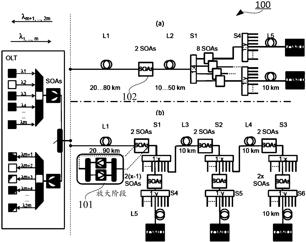
As can be seen from the figure, according to the document "R.Bonk, et al,"Long Reach Passive Optical Network Architectures."In Proceedings of Photonic Networks:15.ITG Symposium,pp.1-5.VDE,2014 "It can be seen that in figure 1 In the structure (b), 2(x-1) semiconductor optical amplifiers are needed, on the one hand, the increase of its quantity brings unfavorable cost and additional energy consumption, and because each SOA semiconductor optical amplifier can only handle Uplink light or downlink light, so the grating must be introduced to separate the uplink and downlink light in the amplification stage, and after processing, it must be mixed through the grating, which introduces additional noise and reduces the transmission performance.

Method used


Image

  • Semiconductor Optical Amplifiers for Optical Communication Systems
  • Semiconductor Optical Amplifiers for Optical Communication Systems
  • Semiconductor Optical Amplifiers for Optical Communication Systems

Examples


Embodiment Construction

[0030] In the following detailed description of the preferred embodiment, reference is made to the accompanying drawings which form a part hereof. The accompanying drawings show, by way of example, specific embodiments in which the invention can be practiced. The illustrated embodiments are not intended to be exhaustive of all embodiments in accordance with the invention. It is to be understood that other embodiments may be utilized and structural or logical changes may be made without departing from the scope of the present invention. Accordingly, the following detailed description is not limiting, and the scope of the invention is defined by the appended claims.

[0031] figure 1 It shows the long-distance passive optical network architecture according to the prior art, since this architecture has been described in the background technology part, it is omitted here to avoid repeated description.

[0032] The present invention proposes a semiconductor optical amplifier use...


PUM

PropertyMeasurementUnit
lengthaaaaaaaaaa
lengthaaaaaaaaaa

Abstract

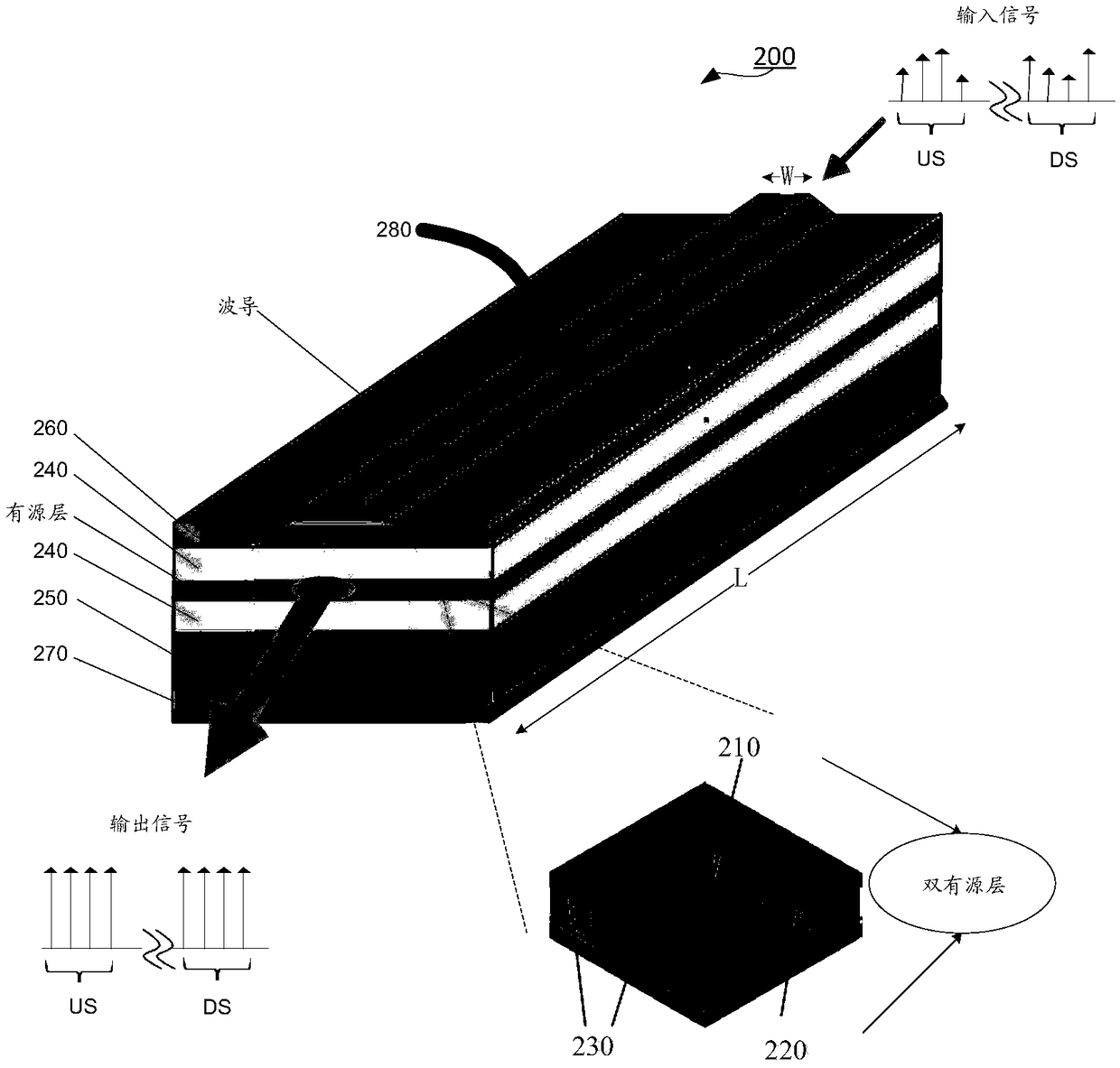
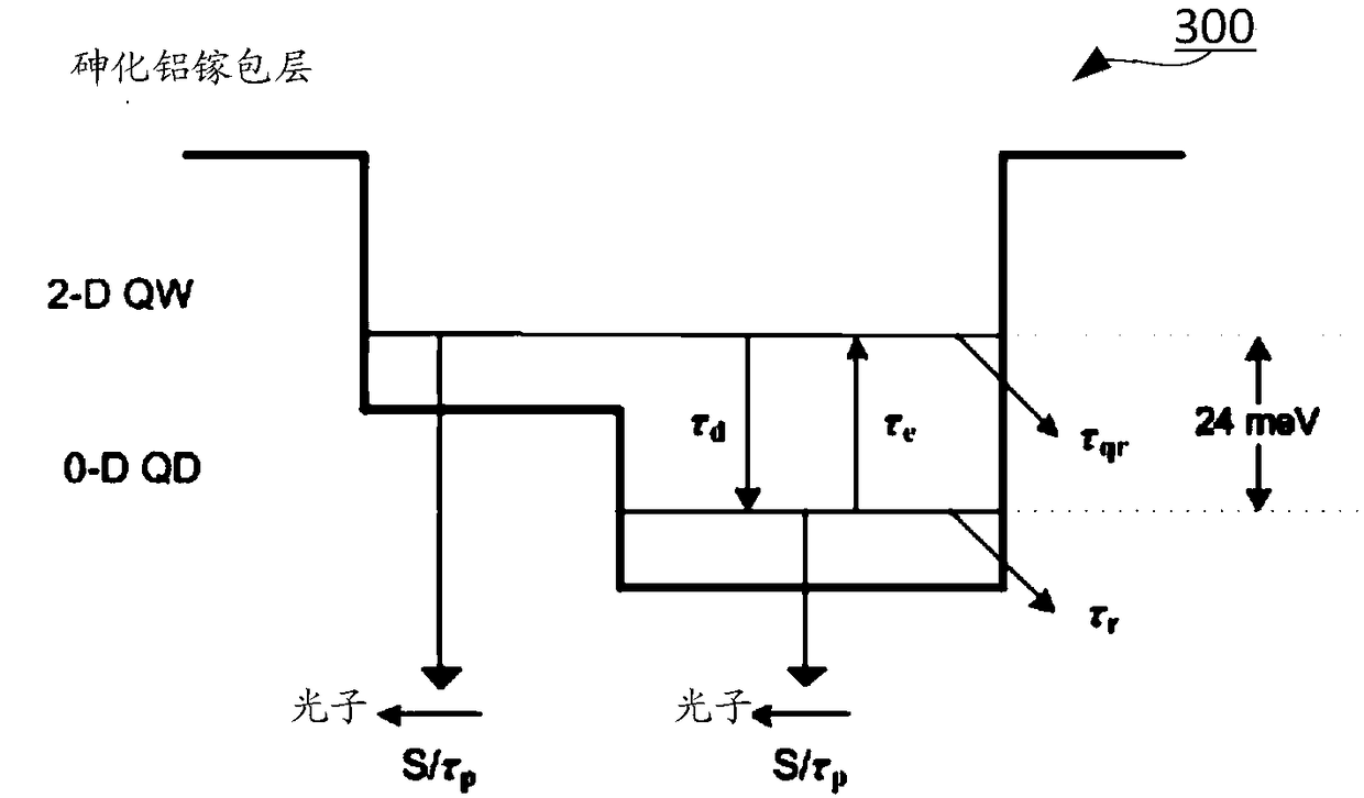
The invention relates to a semiconductor amplifier used for an optical communication system. The semiconductor amplifier is characterized in that an active layer is of a double-active layer structure comprising a first active layer and a second active layer. Profitably, the first active layer is a quantum well layer and the second active layer is a quantum dot layer. According to the invention, 3dB gain bandwidth of the semiconductor amplifier can reach at least 100nm bandwidth, so new design requirements of a time and wavelength division multiplexing passive optical network (TWDM-PON) and a wave division multiplexing passive optical network (WDM-PON). Thus, reuse of the semiconductor amplification of up-and-down signals is achieved, thereby reducing numbers of optical amplifiers and reducing framework cost of the optical amplifiers even the whole passive light network. In addition, power damage caused by a large number of optical amplifiers is reduced, and noise caused by the optical amplifiers is reduced, so signal transmission performance of the whole system is improved.

Description

technical field [0001] The present invention relates to optical communication technology, in particular to a semiconductor optical amplifier used in the optical communication system used in the communication system. Background technique [0002] FSAN and ITU-T have recently announced that the next generation passive optical network NGPON2 should be able to achieve a passive reachable range of more than 40km and its power budget should not be less than 29dB and support a splitting ratio of at least 1:64. Therefore, there is a continuing need for signal amplification of uplink and downlink signals. The wavelength range of the future TWDM-PON is that the upstream wavelength window is in the C-band (1524-1544nm) and the downstream signal wavelength range is in the L+ band (1596-1603nm). On the other hand, wavelength division multiplexed passive optical network (WDM-PON) adopts the full spectrum range including C and L bands, that is, the full band from 1524nm to 1625nm. [000...

Claims


Application Information

Patent Timeline
Patent Type & Authority Patents(China)
IPC IPC(8): H01S3/067G02F1/39
Inventor 孙晓昌庆江
Owner ALCATEL LUCENT SHANGHAI BELL CO LTD
Learn More