
A Programmable Logic Unit Based on AND-OR Structure

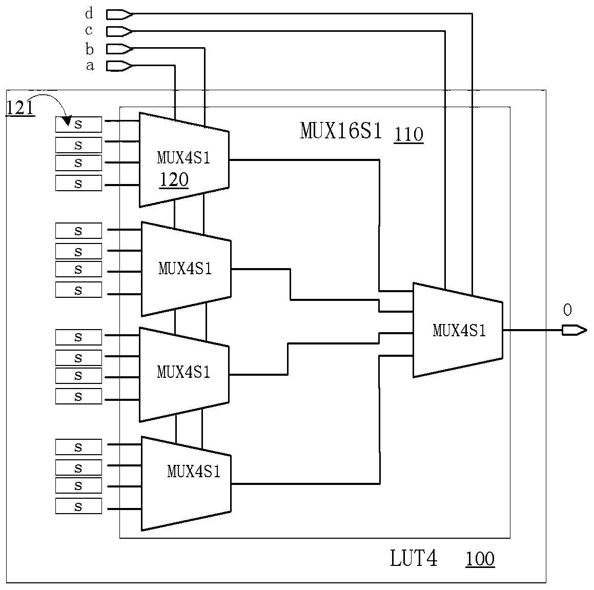
A programming logic and non-structural technology, applied in the field of programmable logic units based on AND or non-structure, can solve the problem of inconvenient application circuit timing constraints, and achieve the effect of small delay difference

Active Publication Date: 2018-09-11
INST OF ELECTRONICS CHINESE ACAD OF SCI
View PDF7 Cites 0 Cited by
  • Summary
  • Abstract
  • Description
  • Claims
  • Application Information

AI Technical Summary

Problems solved by technology

The two configurations have different delay performance on the delay path, which brings inconvenience to the application circuit to realize the later timing constraints

Method used


Image

  • A Programmable Logic Unit Based on AND-OR Structure
  • A Programmable Logic Unit Based on AND-OR Structure
  • A Programmable Logic Unit Based on AND-OR Structure

Examples


Embodiment Construction

[0022] In order to make the object, technical solution and advantages of the present invention clearer, the present invention will be further described in detail below in conjunction with specific embodiments and with reference to the accompanying drawings.

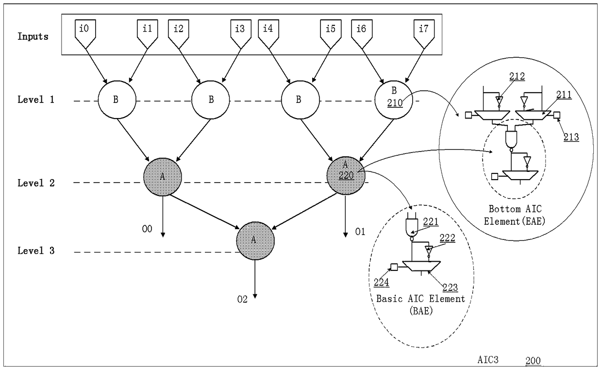
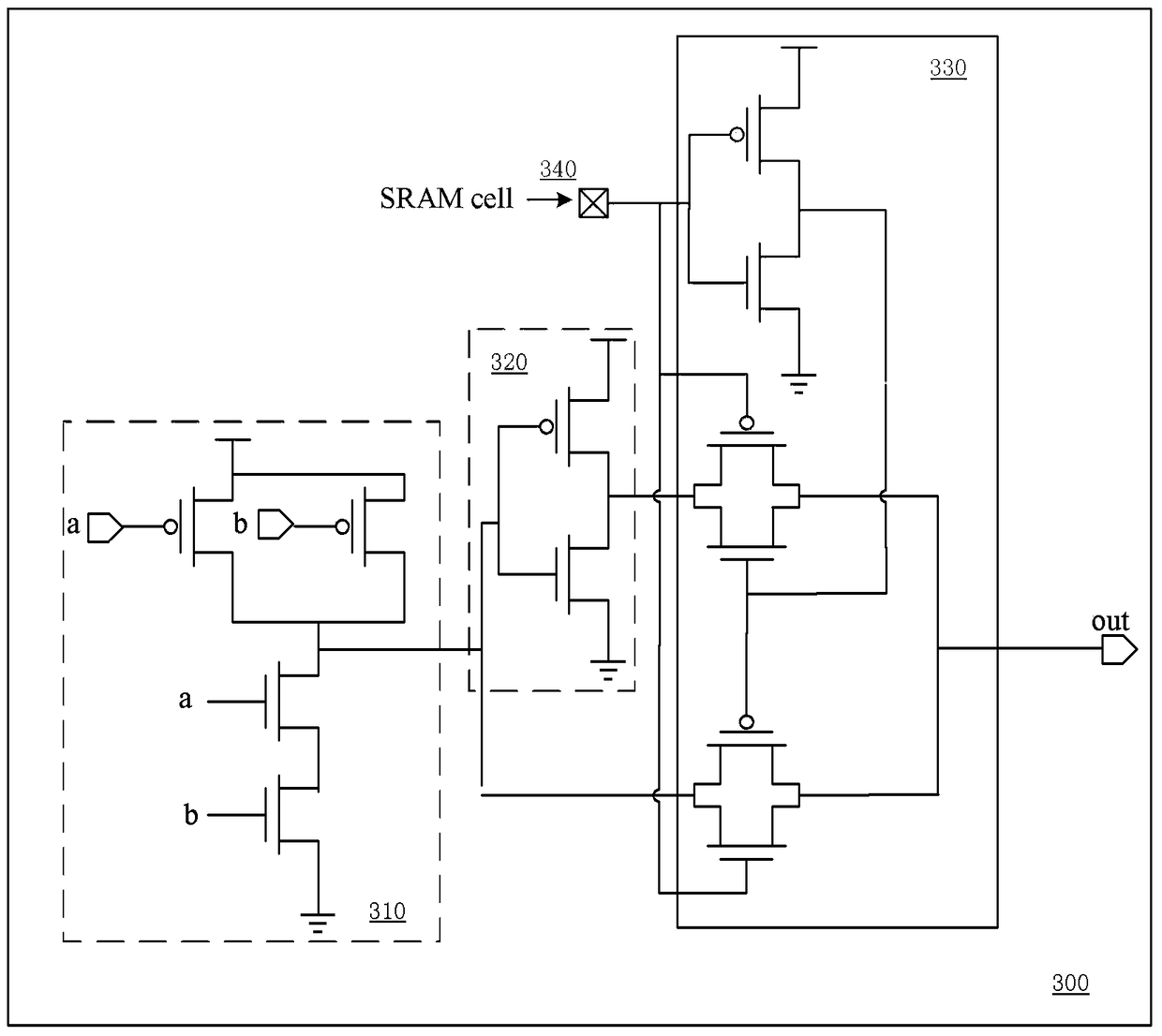
[0023] The present invention proposes a programmable logic unit based on NANDOR (NANDOR) structure, which is used to replace image 3 Shown is the 300 AIC base unit module BAE. The basic working principle of BAE is that it can control the storage value of the SRAM unit through programming to realize the logic function of "AND" or "AND". figure 2 The shown architecture is multi-level connected, that is, complex logic functions can be realized. According to Demogan's theorem, any function can be rewritten into a combined expression of AND and NOT units through logical operations, so the function can be realized through the AIC structure.

[0024] The programmable NANDOR unit (NANDOR) proposed by the present invention can...


PUM


Abstract

The invention discloses a programmable logic element based on a NAND-OR structure. The programmable logic element comprises a NAND-OR basic element; the NAND-OR basic element realizes NAND or NOR functions of first input data and second input data under the control of an output control signal of an SRAM storage element, wherein the NAND-OR basic element comprises a pull-up network pFET logic circuit block and a pull-down network nFET logic circuit block; the pull-up network pFET logic circuit block comprises at least one first to at least one fifth pFET transistors; and the pull-down network nFET logic circuit block comprises at least one first to at least one fifth nFET transistors. According to the invention, programmable NAND-OR is used as a basic AIC element; compared with a AND-inverter cone structure, the NAND-OR structure has the advantages that the series of circuits for a signal to pass through is low; the area is relatively small; the speed is relatively rapid; and the delay difference is relatively low when different functions are realized by adjusting sub-parameters of the transistors.

Description

technical field [0001] The invention belongs to the technical field of computer programmable logic, in particular to a programmable logic unit based on an NANDOR structure. Background technique [0002] Since the development of programmable logic devices, it has become an indispensable medium for the realization of digital circuits. The flexible programmability of programmable devices makes it configurable to implement different logic functions to meet the functional requirements of different users. With the advancement of manufacturing technology, the performance of programmable logic devices has been continuously improved. In addition, programmable logic devices also have a shorter product development time. The above advantages make programmable logic devices widely used in different application fields. [0003] A programmable logic device is mainly composed of a programmable logic block (Configurable Logic Block, CLB) and a programmable interconnection module. The CLB...

Claims


Application Information

Patent Timeline
Patent Type & Authority Patents(China)
IPC IPC(8): H03K19/177
CPCH03K19/17724H03K19/17736
Inventor 黄志洪韦援丰杨立群李威魏星江政泓林郁杨海钢
Owner INST OF ELECTRONICS CHINESE ACAD OF SCI
Learn More