Check patentability & draft patents in minutes with Patsnap Eureka AI!

Array substrate and manufacturing method thereof

A technology of an array substrate and a manufacturing method, which is applied in the display field and can solve problems such as poor touch control of the panel and breakdown of the insulating layer

Active Publication Date: 2019-03-22
SHANGHAI TIANMA MICRO ELECTRONICS CO LTD +1
View PDF5 Cites 0 Cited by
  • Summary
  • Abstract
  • Description
  • Claims
  • Application Information

AI Technical Summary

Problems solved by technology

[0004] In the manufacturing process of the existing touch display panel, there is no electrical connection between the common electrodes 110 (that is, the touch electrodes), and there is no electrical connection between the touch scanning lines corresponding to the common electrodes 110. Therefore, during the production process of the touch display panel, static electricity is likely to be generated between the common electrodes 110. If the accumulated static charge is large, the conductive layer where the touch scanning line is located may be separated from the conductive layer where the common electrode 110 is located. The insulating layer between them is broken down, which leads to the problem of poor touch control of the panel

Method used


Image

  • Array substrate and manufacturing method thereof
  • Array substrate and manufacturing method thereof
  • Array substrate and manufacturing method thereof

Examples


Embodiment Construction

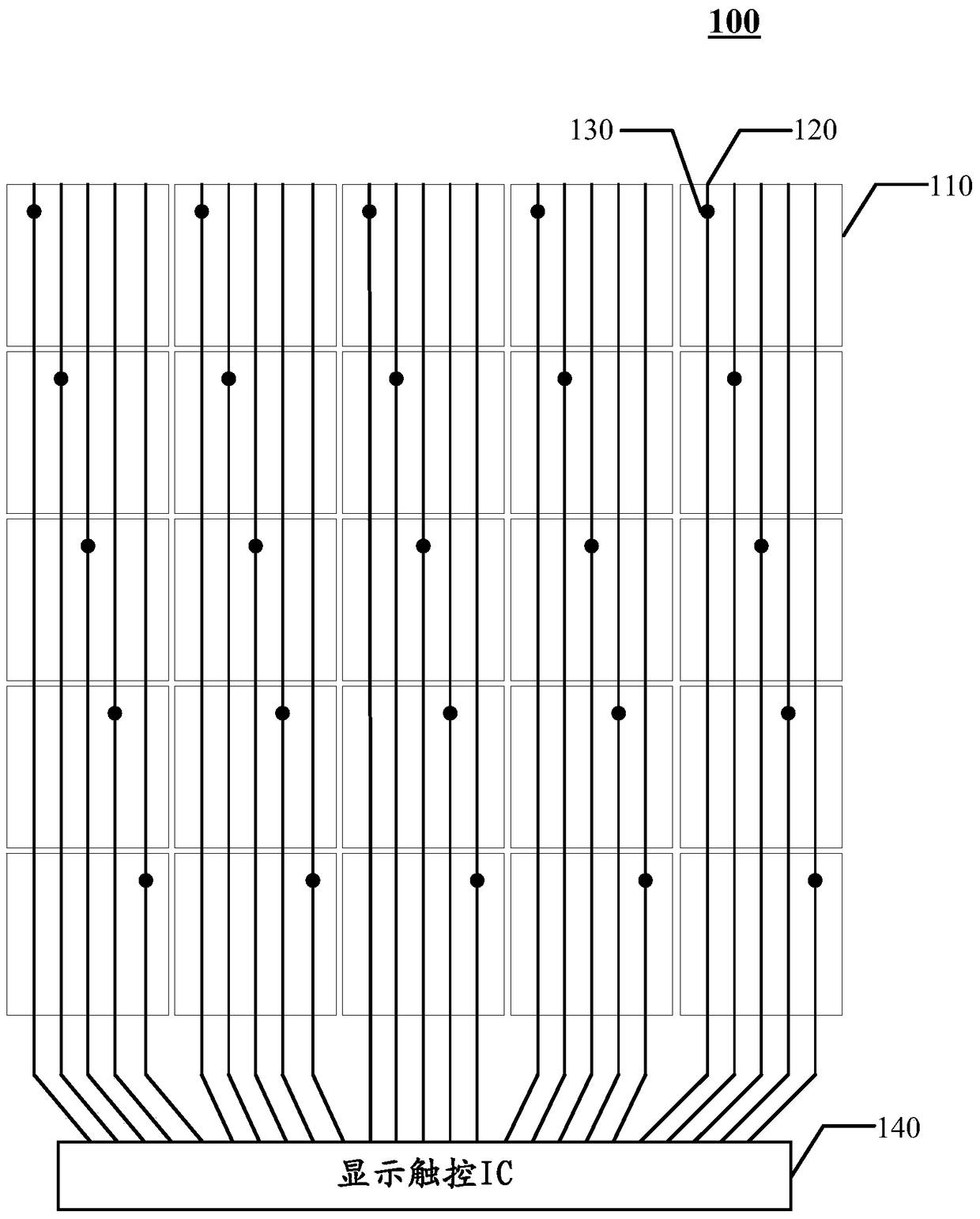
[0021] The application will be further described in detail below in conjunction with the accompanying drawings and embodiments. It should be understood that the specific embodiments described here are only used to explain related inventions, rather than to limit the invention. It should also be noted that, for the convenience of description, only the parts related to the invention are shown in the drawings.

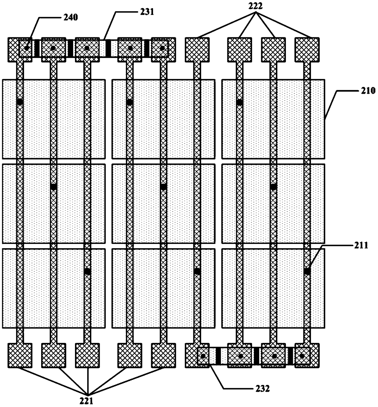
[0022] see figure 2 Shown is a schematic structural diagram of an array substrate according to an embodiment of the present application.

[0023] The array substrate of this embodiment includes: a plurality of common electrodes 210, at least one metal wire cluster ( figure 2 Two metal wire clusters 221 and 222 are schematically shown in . Each metal wire cluster includes a plurality of metal wires, wherein each metal wire is connected to each common electrode 210 in a one-to-one correspondence. In some optional implementation manners, each common electrode 210 and i...


PUM


Abstract

The application discloses an array substrate and a manufacturing method thereof. The array substrate includes a plurality of common electrodes; at least one cluster of metal wires, each cluster of metal wires includes a plurality of metal wires, wherein each metal wire is connected to each common electrode in a one-to-one correspondence; and at least one conductor block group, each conductor The block group includes at least one conductor block, and each conductor block group corresponds to each metal wire cluster; wherein, the conductor block includes at least two conductive parts, and openings are provided between adjacent conductive parts to insulate adjacent conductive parts, Each conductive portion is electrically connected to one metal wire in the corresponding metal wire cluster. According to the solution of the present application, it is possible to prevent static electricity from being generated between the common electrodes during the manufacturing process of the array substrate, thereby affecting touch control and / or display effects.

Description

technical field [0001] The present disclosure generally relates to the field of display technology, and in particular, relates to an array substrate and a manufacturing method thereof. Background technique [0002] Existing touch display panels include a plurality of block-shaped common electrodes arranged in an array, and these block-shaped common electrodes can be reused as touch electrodes in the touch scanning stage. Each touch electrode is electrically connected to one end of a touch scan line, and the other end of the touch scan line is connected to the display touch chip for receiving and sending touch scan signals to the touch electrodes. [0003] Such as figure 1 As shown in FIG. 2 , it is a schematic structural diagram of an embodiment of an existing touch display panel. Wherein, reference numeral 110 is a block-shaped common electrode, and the block-shaped common electrode 110 can be electrically connected to one end of the touch scanning line 120 through the vi...

Claims


Application Information

Patent Timeline
Patent Type & Authority Patents(China)
IPC IPC(8): H01L27/32H01L27/12H01L21/77
CPCH01L27/124H10K59/00H10K59/40
Inventor 丁洪周星耀
Owner SHANGHAI TIANMA MICRO ELECTRONICS CO LTD
Features
  • R&D
  • Intellectual Property
  • Life Sciences
  • Materials
  • Tech Scout
  • Unparalleled Data Quality
  • Higher Quality Content
  • 60% Fewer Hallucinations
Learn More