Check patentability & draft patents in minutes with Patsnap Eureka AI!

A kind of terahertz semiconductor laser and its manufacturing method

A laser and semiconductor technology, applied in the field of terahertz band light sources, can solve the problems affecting the heat dissipation of the active area of ​​the device, and it is difficult to realize flip-chip welding of the laser, and achieve the effect of improving the emission efficiency and beam quality, and improving the heat dissipation.

Active Publication Date: 2018-11-27
INST OF SEMICONDUCTORS - CHINESE ACAD OF SCI
View PDF7 Cites 0 Cited by
  • Summary
  • Abstract
  • Description
  • Claims
  • Application Information

AI Technical Summary

Problems solved by technology

But on the other hand, this structure makes the upper and lower electrodes of the laser on the same side, and the laser is difficult to achieve flip-chip welding during packaging, and the thicker substrate affects the heat dissipation of the active area of ​​the device.

Method used


Image

  • A kind of terahertz semiconductor laser and its manufacturing method
  • A kind of terahertz semiconductor laser and its manufacturing method
  • A kind of terahertz semiconductor laser and its manufacturing method

Examples


Embodiment Construction

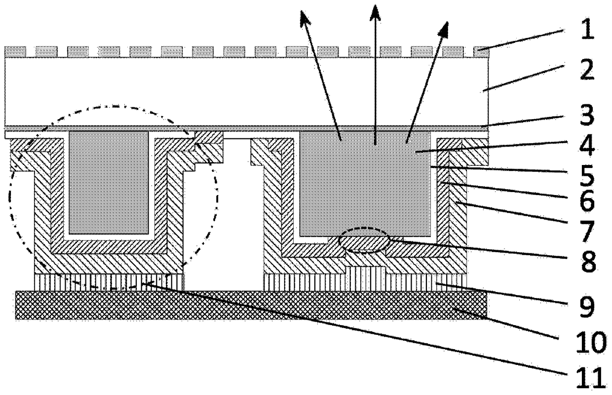
[0033] In order to make the object, technical solution and advantages of the present invention clearer, the present invention will be further described in detail below in conjunction with specific embodiments and with reference to the accompanying drawings. It should be noted that "up", "down", "inside" and "outside" in the present invention are only used to indicate the relative positional relationship between each layer relative to the reference plane, and are not used to indicate the actual up and down and inside and outside relationship, the actual components can be installed in forward or reverse order according to specific needs.

[0034] Terahertz semiconductor lasers have great application prospects as a small, high-efficiency coherent terahertz light source. In order to achieve large power output, a semi-insulating plasmonic waveguide structure is usually used. For such terahertz lasers, heat accumulation in the active region caused by high current injection is one o...


PUM


Abstract

The invention relates to a terahertz semiconductor laser and a manufacturing method thereof. The terahertz semiconductor laser comprises a metal sub-wavelength grating layer, a semi-insulating substrate layer, a high-doped semiconductor layer and two table facets with same structures, wherein the two table facets are formed by deeply corroding an epitaxial layer; one of the table facets serves as an active area structure of the laser while the other table facet serves as a supporting table facet for a lower electrode; the functions of the two table facets are realized by only controlling the injection of the current through graph difference of an insulating layer. The terahertz semiconductor laser is based on an active-area horizontal area-selecting electroplating auxiliary radiating metal layer and imaging heat sinking flip-chip structure which can be used for improving the heat dissipation property of the active area of the component and conveniently forming substrate surface emission, so that the terahertz laser emission efficiency and light beam quality are increased.

Description

technical field [0001] The invention relates to the technical field of terahertz band light sources, in particular to a terahertz semiconductor laser and a manufacturing method thereof. Background technique [0002] Terahertz quantum cascade laser is a small, high-efficiency terahertz semiconductor laser source, which has important potential applications in astronomy, biomedicine, environmental science, safety detection, free space optical communication, etc. focus on. High output power, high operating temperature and good beam characteristics have always been important issues to be solved in the research of terahertz semiconductor lasers. Terahertz semiconductor lasers mainly use two waveguide structures: double-sided metal waveguides and semi-insulating plasma waveguides. Due to the high optical confinement factor of the double-sided metal waveguide structure, the lasing threshold of the laser is reduced, the injection power consumption is reduced, and the operating temp...

Claims


Application Information

Patent Timeline
Patent Type & Authority Patents(China)
IPC IPC(8): H01S5/00H01S5/02H01S5/024
CPCH01S5/00H01S5/02H01S5/024
Inventor 刘俊岐王涛李媛媛刘峰奇王利军张锦川翟慎强刘舒曼卓宁王占国
Owner INST OF SEMICONDUCTORS - CHINESE ACAD OF SCI
Features
  • R&D
  • Intellectual Property
  • Life Sciences
  • Materials
  • Tech Scout
  • Unparalleled Data Quality
  • Higher Quality Content
  • 60% Fewer Hallucinations
Learn More