

Manufacturing method of transistor and transistor
A manufacturing method and transistor technology, applied in the direction of transistors, semiconductor/solid-state device manufacturing, electric solid-state devices, etc., can solve the problems of plating layer peeling, swelling, weak adhesion of the plating film, etc., and achieve the effect of stable action behavior
- Summary
- Abstract
- Description
- Claims
- Application Information
AI Technical Summary
Problems solved by technology
Method used
Image

Examples
Embodiment 1
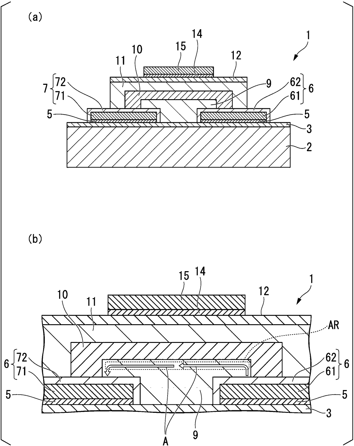
[0133] (Fabrication of source and drain)
[0134] In this example, 3-aminopropyltriethoxysilane (KBE903, manufactured by Shin-Etsu Silicone Co., Ltd.), which is an amine-based silane coupling agent, was dissolved in methyl isobutyl ketone ( Hereinafter, sometimes referred to as MIBK), to prepare a liquid for the formation of basement membrane.
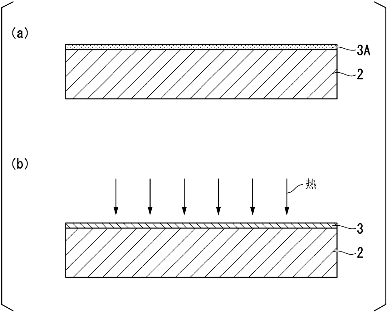
[0135] After the surface of a PET substrate (model: A-4100 (uncoated), manufactured by Toyobo Co., Ltd.) was cleaned with atmospheric pressure oxygen plasma, the above liquid was applied to the PET substrate by dip coating. The pulling speed of the dip coating was 1 mm / sec. Then, it heated at 105 degreeC for 15 minutes, and formed the base film.
[0136] Next, hexamethyldisilazane (12058-1A, manufactured by Kanto Chemical Co., Ltd.) was coated on the PET substrate on which the base film was formed by dip coating (pulling speed: 1 mm / sec). Thereafter, it was heated at 105° C. for 10 minutes to form a protective layer.
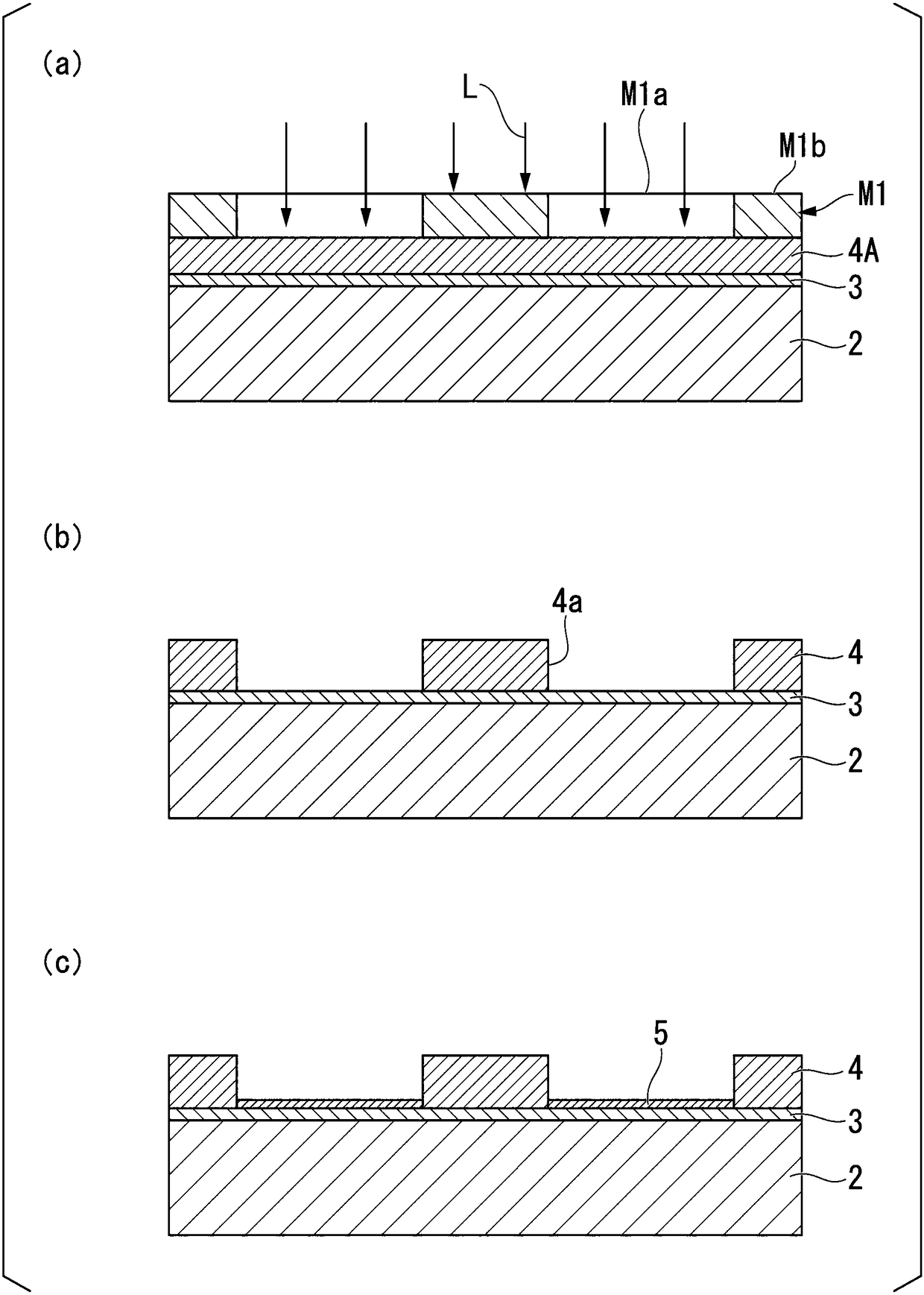
[0137] Next,...
PUM
| Property | Measurement | Unit |
|---|---|---|
| particle size | aaaaa | aaaaa |
| thickness | aaaaa | aaaaa |
Abstract
Description
Claims
Application Information