Image acquisition device for detecting concentricity between led chip and lens

A LED chip and image acquisition technology, applied in the direction of measuring devices, optical devices, instruments, etc., can solve the problems of LED chip light emission (chromaticity, luminance unevenness, lower product yield, etc., to achieve product yield improvement, The effect of improving production efficiency and reducing production cost

Active Publication Date: 2019-05-17
SUZHOU PINBO ELECTRONICS TRADING CO LTD
View PDF6 Cites 0 Cited by
  • Summary
  • Abstract
  • Description
  • Claims
  • Application Information

AI Technical Summary

Problems solved by technology

If the concentricity between the LED chip and the lens is large, then the subsequent production of the light-emitting module will produce non-uniform light emission (chromaticity, luminance) between the LED chips during work, and even the lens and other components to be assembled Interference between parts occurs, which will reduce product yield
There is currently no detection scheme for the concentricity between the LED chip and the lens in the prior art, so how to quickly detect the concentricity between the LED chip and the lens during production, so that unqualified products can be quickly discharged to improve product qualification Efficiency and cost reduction, this is just the problem that the inventor will solve

Method used


Image

  • Image acquisition device for detecting concentricity between led chip and lens
  • Image acquisition device for detecting concentricity between led chip and lens
  • Image acquisition device for detecting concentricity between led chip and lens

Examples


Embodiment Construction

[0013] The present invention will be further described below in conjunction with accompanying drawing.

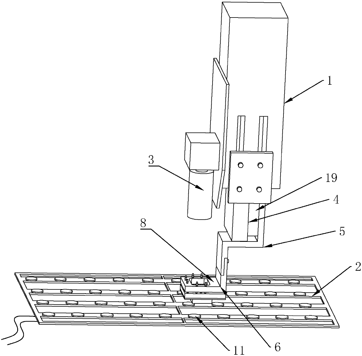
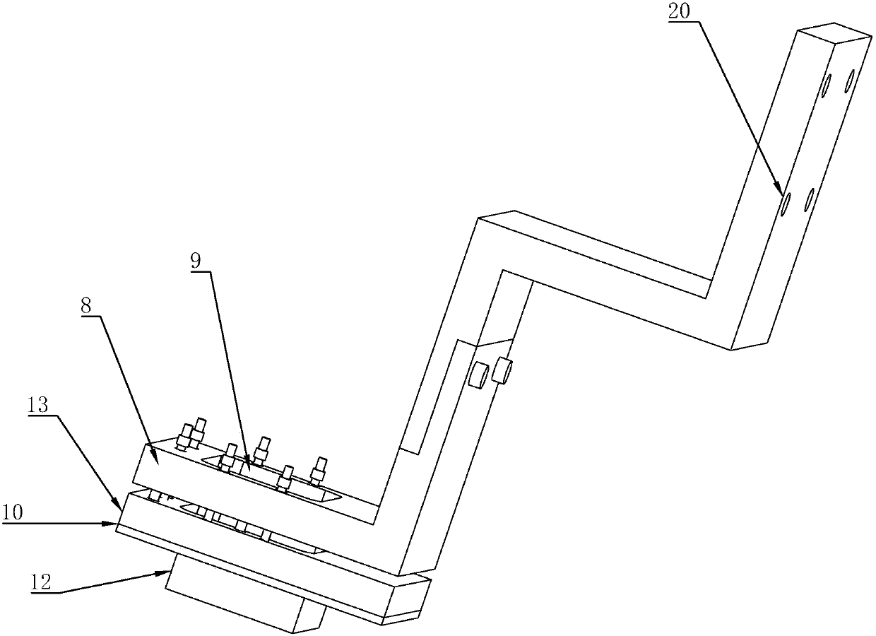
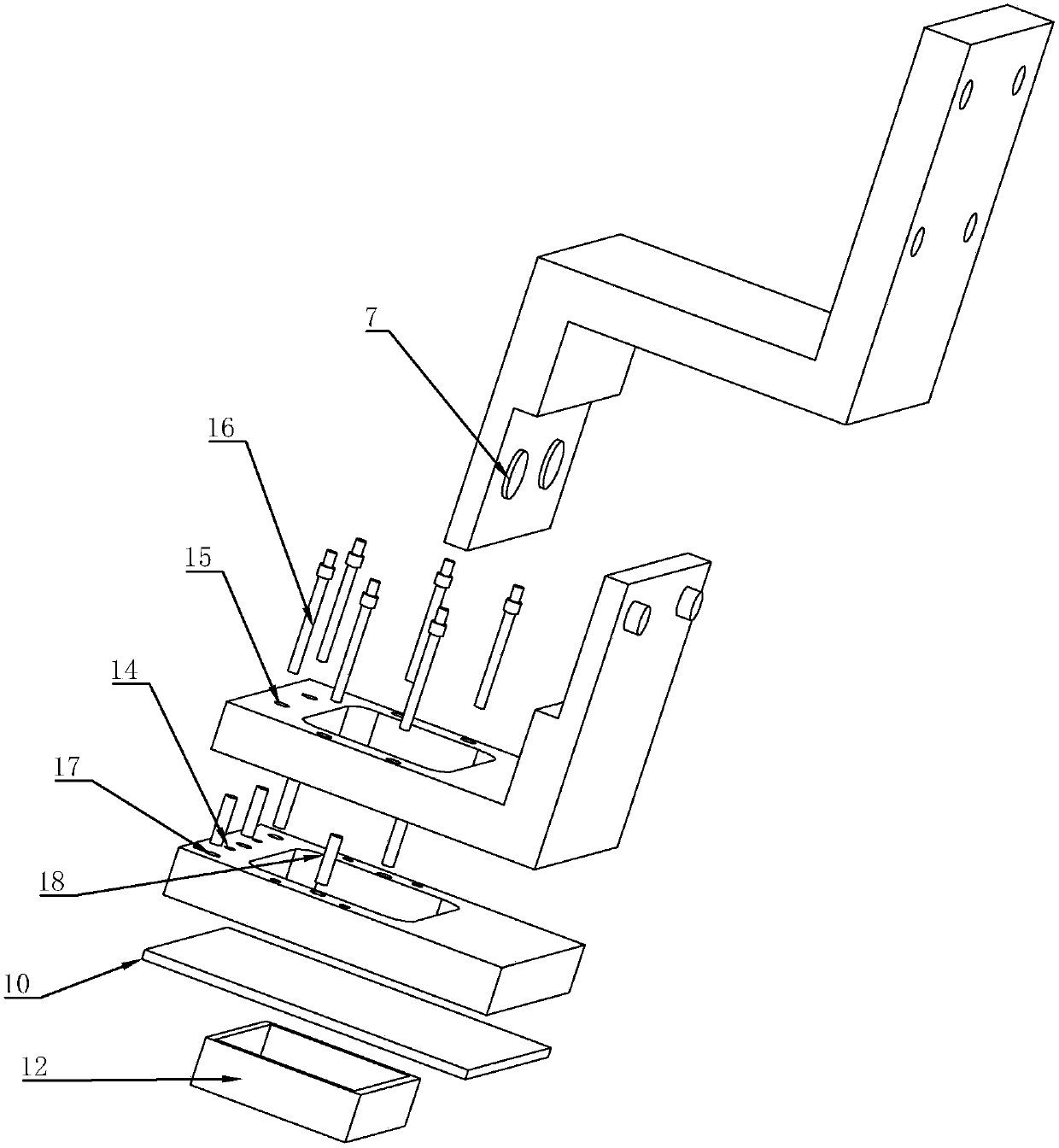
[0014] Such as Figure 1 to Figure 3 As shown, an image acquisition device for detecting the concentricity between the LED chip and the lens includes a base 1 capable of moving up, down, left, and right, the base 1 is located above the LED chip module 2, and the LED chip module 2 is powered on and emits light. The base 1 is provided with a mounting block 4 and an image acquisition mechanism 3, the mounting block 4 is detachably provided with a first bracket 5, the first bracket 5 is connected with a second bracket 6, and the first bracket 5 is provided with a first magnet 7 , the second bracket 6 is provided with a second magnet that attracts each other with the first magnet 7, the first bracket 5 and the second bracket 6 are connected by the attractive force between the first magnet 7 and the second magnet, and the second bracket 6 is provided with a mounting part 8 locat...


PUM


Abstract

The invention discloses an image acquisition device for detecting concentricity between LED chips and lenses. According to the technical scheme, the image acquisition device comprises a base which can move up and down and left and right and is positioned above an LED chip module, wherein the LED chips give out light after being electrified, an installation block and an image acquisition mechanism are arranged on the base, a first support is detachably arranged on the installation block, a first magnet is arranged on the first support, a second magnet is arranged on a second support, the second magnet and the first magnet attract with each other, the first support and the second support are connected via attraction force between the first magnet and the second magnet, an installation part just below the image acquisition mechanism is arranged on the second support, and a diffusion plate covering a light transmission hole is arranged below the installation part. The image acquisition device fills up the technical blank in the field of lens type illumination module detection, and can be used for greatly lowering production cost of lens type illumination modules, improving the quality rate of the modules and improving the production efficiency when applied to production of the lens type illumination modules.

Description

technical field [0001] The invention relates to an image acquisition device for detecting the concentricity between an LED chip and a lens in a lens type light emitting module. Background technique [0002] The general structure of the light-emitting module used in the display usually includes LED chips mounted on the PCB by SMT, and then a lens is added to each LED chip to form the LED chip module. If the concentricity between the LED chip and the lens is large, then the subsequent production of the light-emitting module will produce non-uniform light emission (chromaticity, luminance) between the LED chips during work, and even the lens and other components to be assembled Interference between parts occurs, which reduces product yield. There is currently no detection scheme for the concentricity between the LED chip and the lens in the prior art, so how to quickly detect the concentricity between the LED chip and the lens during production, so that unqualified products ca...

Claims


Application Information

Patent Timeline
Patent Type & Authority Patents(China)
IPC IPC(8): G01B11/27
CPCG01B11/27
Inventor 李柏蓉
Owner SUZHOU PINBO ELECTRONICS TRADING CO LTD
Why Eureka
Try Eureka