A light-emitting diode chip and its manufacturing method

A technology for light-emitting diodes and a manufacturing method, which is applied to electrical components, circuits, semiconductor devices, etc., can solve the problems of low reflectivity of non-vertically incident light, low luminous efficiency of LED chips, etc., to improve stability, improve luminous brightness and luminous The effect of efficiency

Active Publication Date: 2018-05-22
HC SEMITEK CORP
View PDF8 Cites 0 Cited by
  • Summary
  • Abstract
  • Description
  • Claims
  • Application Information

AI Technical Summary

Problems solved by technology

[0006] In order to solve the problem of low reflectance of DBR for non-perpendicularly incident light in the prior art, resulting in low luminous efficiency of LED chips, an embodiment of the present invention provides a light emitting diode chip and a manufacturing method thereof

Method used


Image

  • A light-emitting diode chip and its manufacturing method
  • A light-emitting diode chip and its manufacturing method
  • A light-emitting diode chip and its manufacturing method

Examples


Embodiment 1

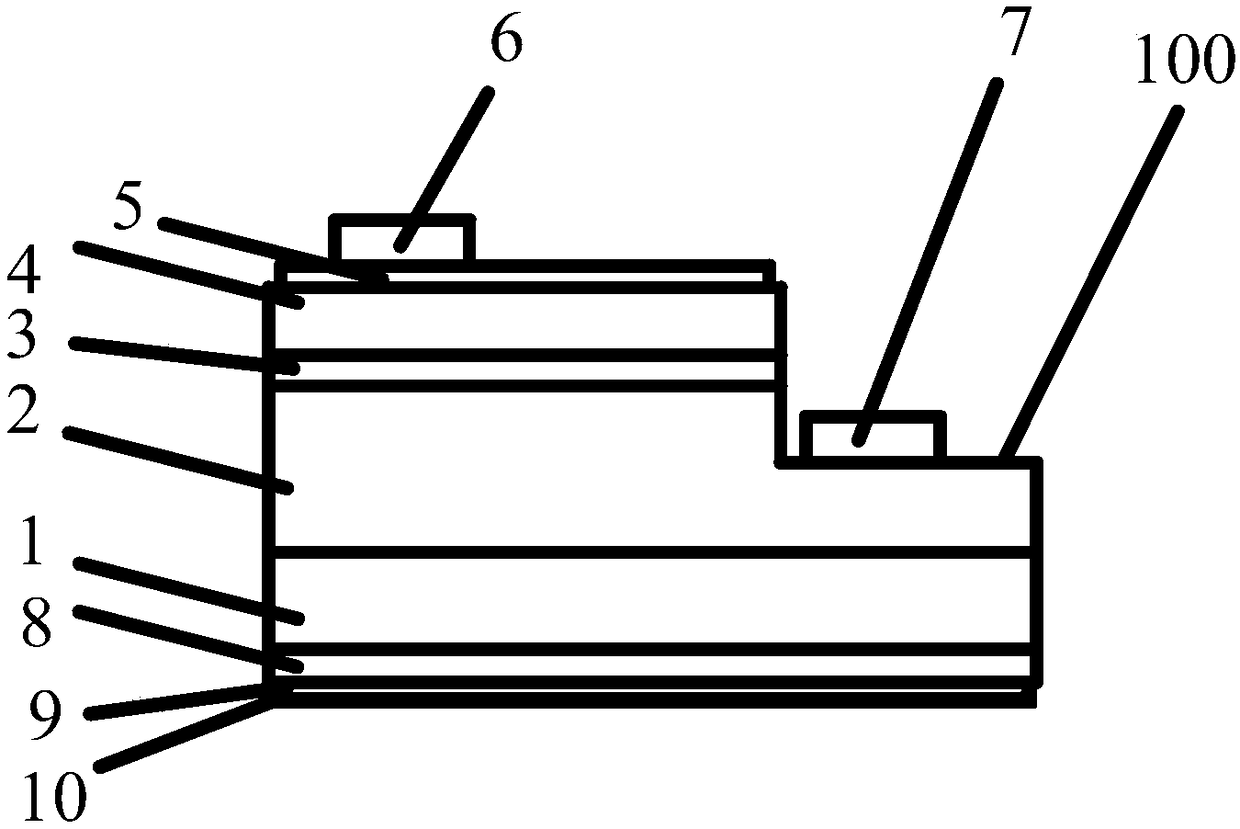
[0036] An embodiment of the present invention provides a light emitting diode chip, see figure 1 , the light-emitting diode chip includes a substrate 1, an N-type layer 2, a light-emitting layer 3, a P-type layer 4, a transparent conductive film (TCO) 5, a P-type electrode 6, an N-type electrode 7, a DBR 8, and an Ag metal reflective layer 9 and metal protective layer 10, N-type layer 2, light-emitting layer 3, and P-type layer 4 are sequentially stacked on the first surface of substrate 1, and P-type layer 4 is provided with a concave hole extending from P-type layer 4 to N-type layer 2. The groove 100, the transparent conductive film 5 and the P-type electrode 6 are sequentially arranged on the P-type layer 4, the N-type electrode 7 is arranged on the N-type layer 2, and the DBR 8, the Ag metal reflective layer 9, and the metal protection layer 10 are sequentially arranged on the substrate. On the second surface of the bottom 1, the metal protective layer 10 and the DBR 8 fo...

Embodiment 2

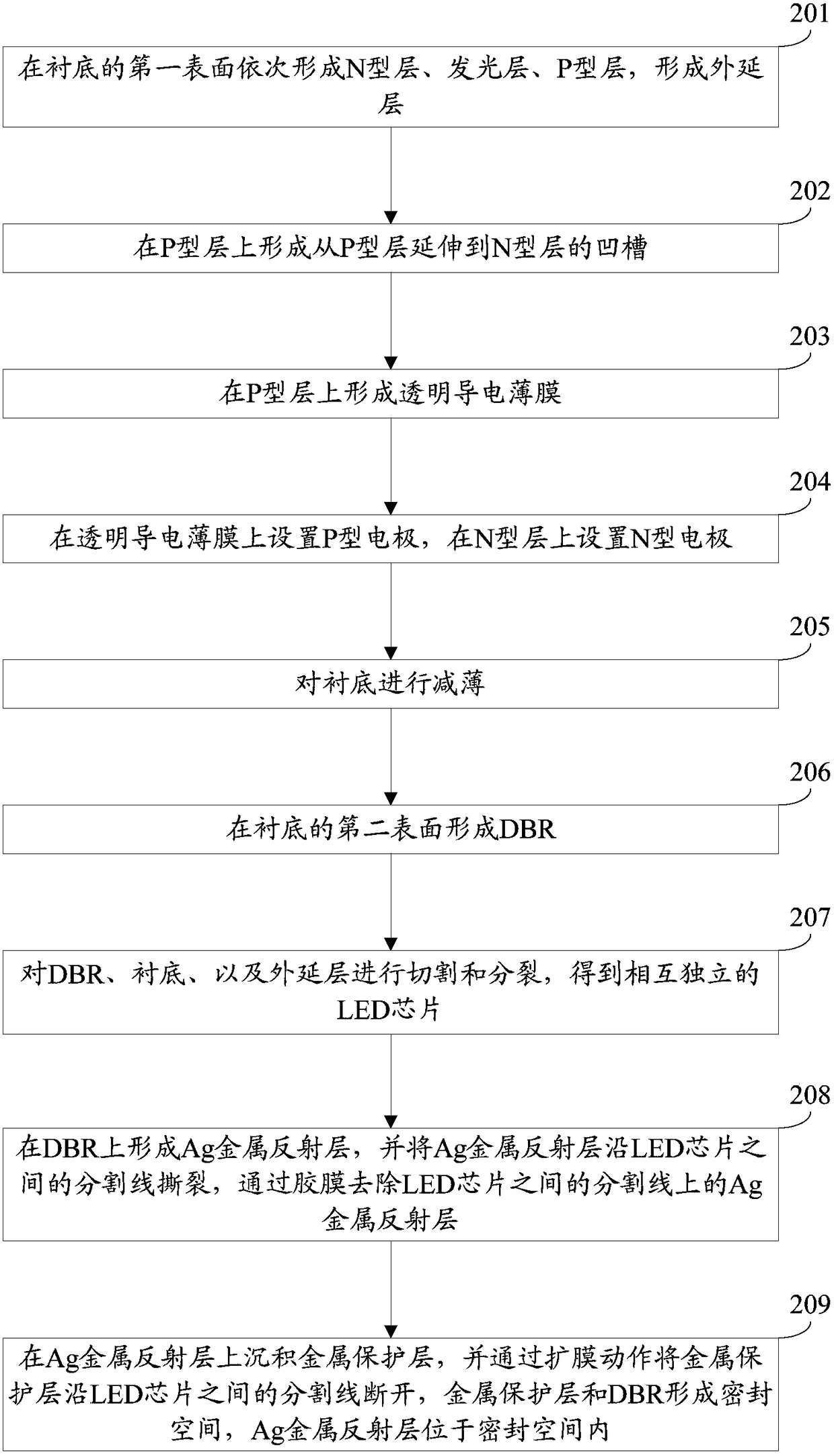
[0048] An embodiment of the present invention provides a method for manufacturing a light emitting diode chip, see figure 2 , the production method includes:

[0049] Step 201: sequentially forming an N-type layer, a light-emitting layer, and a P-type layer on the first surface of the substrate to form an epitaxial layer.

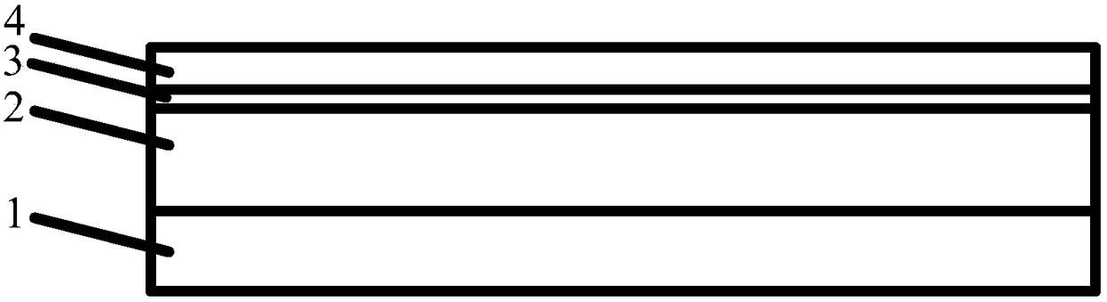
[0050] Figure 3a It is a schematic structural diagram of the LED chip after step 201 is performed. Wherein, 1 is a substrate, 2 is an N-type layer, 3 is a light-emitting layer, and 4 is a P-type layer.

[0051]In this embodiment, the N-type layer may be an N-type GaN layer, the light emitting layer may be alternately stacked InGaN layers and GaN layers, and the P-type layer may be a P-type GaN layer.

[0052] Optionally, the substrate may be one of a flat-surfaced sapphire substrate, a patterned sapphire substrate (Patterned Sapphire Substrate, PSS for short), a Si substrate, a GaN substrate, a SiN substrate, a SiC substrate, and a glass substrate. sp...


PUM


Abstract

The invention discloses a light-emitting diode chip and a manufacturing method thereof, belonging to the technical field of semiconductors. The light-emitting diode chip includes a substrate, an N-type layer, a light-emitting layer, a P-type layer, a transparent conductive film, a P-type electrode, an N-type electrode, and a DBR, and the N-type layer, the light-emitting layer, and the P-type layer are sequentially stacked on the substrate The first surface of the P-type layer is provided with a groove extending from the P-type layer to the N-type layer. The transparent conductive film and the P-type electrode are arranged on the P-type layer in turn, and the N-type electrode is arranged on the N-type layer. DBR It is arranged on the second surface of the substrate, the second surface is the surface opposite to the first surface, and the light-emitting diode chip further includes an Ag metal reflective layer and a metal protection layer stacked on the DBR in sequence, and the metal protection layer and the DBR form a sealed space, The Ag metal reflective layer is located in the sealed space. The invention can realize all-round reflection and improve the luminous brightness and luminous efficiency of the light-emitting diode.

Description

technical field [0001] The invention relates to the technical field of semiconductors, in particular to a light emitting diode chip and a manufacturing method thereof. Background technique [0002] Light Emitting Diode (LED for short) is a semiconductor diode that can convert electrical energy into light energy. [0003] The existing LED chip includes an N-type layer, a light-emitting layer, and a P-type layer stacked on the first surface of the substrate in sequence, and the P-type layer is provided with a groove extending from the P-type layer to the N-type layer, a transparent conductive film and The P-type electrodes are sequentially disposed on the P-type layer, the N-type electrodes are disposed on the N-type layer, and the second surface of the substrate is provided with a Distributed Bragg Reflection (Distributed Bragg Reflection, DBR for short). Wherein, the second surface is the surface opposite to the first surface. [0004] In the process of realizing the prese...

Claims


Application Information

Patent Timeline
Patent Type & Authority Patents(China)
IPC IPC(8): H01L33/46H01L33/00
CPCH01L33/005H01L33/46
Inventor 尹灵峰王江波
Owner HC SEMITEK CORP
Why Eureka
Try Eureka