Eureka AIR delivers breakthrough ideas for toughest innovation challenges, trusted by R&D personnel around the world.

OLED and its preparation method, and OLED display device

A technology of confinement layer and organic material layer, which is applied in semiconductor/solid-state device manufacturing, organic semiconductor devices, electrical components, etc., can solve problems affecting OLED device injection efficiency, lifespan, OLED device damage, large energy, etc., and achieve manufacturing process Simple, Brightness and Uniformity Improvement, Effect of Uniformity Improvement

Active Publication Date: 2018-09-07
BOE TECH GRP CO LTD
View PDF7 Cites 0 Cited by
  • Summary
  • Abstract
  • Description
  • Claims
  • Application Information

AI Technical Summary

Problems solved by technology

However, since the transparent metal oxide material needs to be prepared by a process such as sputtering, the energy during sputtering is relatively large, and it is easy to cause damage to the OLED device, which in turn affects the performance of the OLED device such as injection efficiency and lifetime.

Method used


Image

  • OLED and its preparation method, and OLED display device
  • OLED and its preparation method, and OLED display device
  • OLED and its preparation method, and OLED display device

Examples


Embodiment Construction

[0031]In order to make the purpose, technical solutions and advantages of the embodiments of the present invention clearer, the technical solutions in the embodiments of the present invention will be clearly and completely described below in conjunction with the drawings in the embodiments of the present invention. Obviously, the described embodiments It is a part of embodiments of the present invention, but not all embodiments. Based on the embodiments of the present invention, all other embodiments obtained by persons of ordinary skill in the art without creative efforts fall within the protection scope of the present invention.

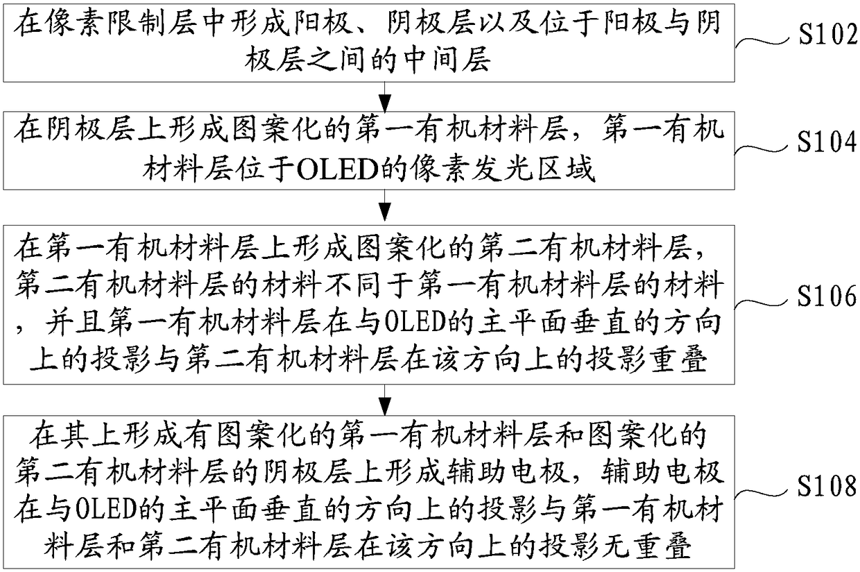
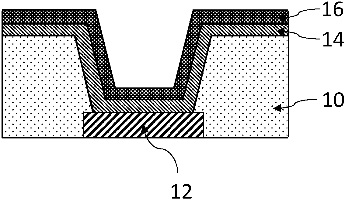
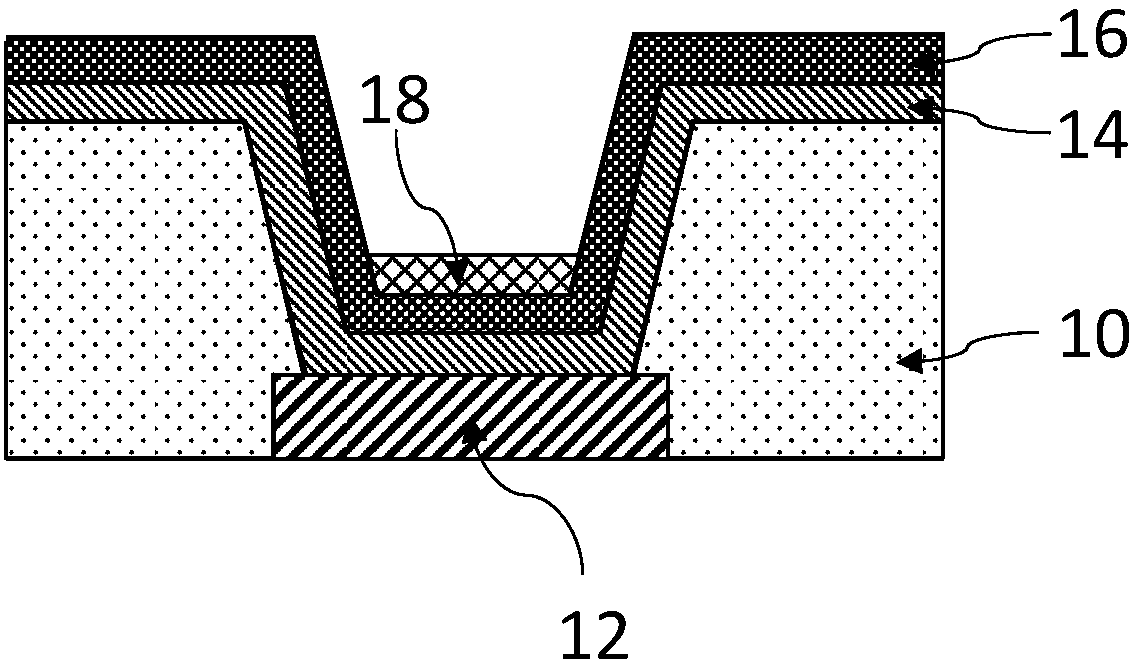
[0032] According to exemplary embodiments of the present invention, there are provided an OLED, a manufacturing method thereof, and an OLED display device.

[0033] figure 1 is a flow chart of preparing OLED according to the embodiment of the present invention. like figure 1 Shown, the preparation method of this OLED comprises:

[0034] Step S1...


PUM

PropertyMeasurementUnit
refractive indexaaaaaaaaaa

Abstract

Embodiments of the present invention relate to OLEDs, methods for preparing the same, and OLED display devices. The preparation method of the OLED includes: forming an anode, a cathode layer, and an intermediate layer between the anode and the cathode layer in the pixel limiting layer; forming a patterned first organic material layer on the cathode layer, and the first organic material layer is located in the OLED The pixel light-emitting area; on the first organic material layer, a patterned second organic material layer is formed, wherein the material of the second organic material layer is different from the material of the first organic material layer, and the first organic material layer is in the same shape as the OLED The projection in the direction perpendicular to the main plane overlaps with the projection of the second organic material layer in this direction; and the patterned first organic material layer and the patterned second organic material layer are formed on the cathode layer. An auxiliary electrode, wherein the projection of the auxiliary electrode in a direction perpendicular to the main plane of the OLED does not overlap with the projections of the first organic material layer and the second organic material layer in this direction.

Description

technical field [0001] Embodiments of the present invention generally relate to the fields of organic light-emitting display and lighting, and particularly relate to large-scale OLEDs, their preparation methods, and OLED display devices. Background technique [0002] Current active organic light-emitting diode (OLED) devices are generally controlled by thin-film transistors (TFTs). Therefore, if the OLED device of the bottom emission structure emits light in the form of bottom emission, the light emitted from the bottom will be blocked by the TFT and metal wire circuits formed on the substrate when passing through the substrate, so the actual light emitting area is limited, and the reduction can be reduced. The ratio of the light-emitting area is the so-called aperture ratio. In addition, in order to improve the luminance difference between pixels, many current OLEDs under research adopt a circuit-compensated pixel structure, and in these pixel structures, for example, a pi...

Claims


Application Information

Patent Timeline
Patent Type & Authority Patents(China)
IPC IPC(8): H01L51/52H01L51/56H01L27/32
CPCH10K59/122H10K50/824H10K2102/3026H10K71/00H10K71/166H10K50/85H10K50/15H10K50/16H10K50/81H10K50/828
Inventor 张粲高雪
Owner BOE TECH GRP CO LTD
Why Eureka
Eureka Blog
Learn More