
Eureka
For R&D, Eureka makes reading and utilizing patents & technical documents easy.
Eureka AIR
Designed for self-driven R&D workflows. Generate viable solutions, solve complex R&D challenges, empower your innovation with AI.

Eureka Materials
Designed for material experts only. Revolutionize your material R&D, from search, analyze, to developing new materials.

TechResearch
Generate reliable direction feasibility study reports for your R&D in just a few steps.

TechSeek
Discover and master advanced knowledge NOW. Basics, ideas, possibilities, all at once.

TechMind
As an expert in R&D Theories, TechMind can generates customized viable solutions instantly.

TechRisk
Analyze your overall solution with one click, know your potential R&D risks in advance.

TechMonitor
Get weekly tech updates, stay abreast of the latest tech innovations and key insights.
Organic light emitting diode display and manufacturing method thereof
A technology for light-emitting diodes and a manufacturing method, which is applied to semiconductor devices, electric solid-state devices, electrical components, etc., can solve the problems of insufficient brightness uniformity, large distance, and long lines, and achieves elimination of insufficient brightness uniformity and reduction of resistance voltage drop. Effect
- Summary
- Abstract
- Description
- Claims
- Application Information
AI Technical Summary
Problems solved by technology
Method used
Image

Examples
Embodiment Construction
[0021] The following descriptions of the various embodiments refer to the accompanying drawings to illustrate specific embodiments in which the present invention can be practiced. Furthermore, the directional terms mentioned in the present invention are, for example, up, down, top, bottom, front, back, left, right, inside, outside, side, surrounding, central, horizontal, transverse, vertical, longitudinal, axial, The radial direction, the uppermost layer or the lowermost layer, etc. are only directions referring to the attached drawings. Therefore, the directional terms used are used to illustrate and understand the present invention, but not to limit the present invention.
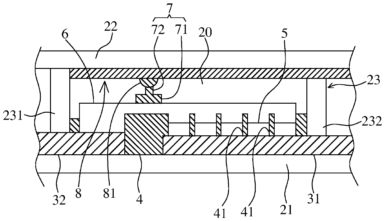
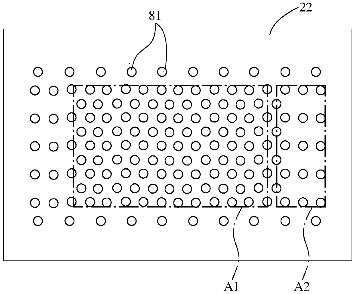
[0022] Please refer to figure 1 Shown is a schematic diagram of a preferred embodiment of the organic light emitting diode display of the present invention. The OLED display includes a substrate 21, an anode conductive layer 31, a cathode conductive layer 32, a pixel definition layer 4, an organic lumin...
PUM
 Abstract
Description
Claims
Application Information
 - R&D Engineer
- R&D Manager
- IP Professional
- Industry Leading Data Capabilities
- Powerful AI technology
- Patent DNA Extraction
Browse by: Latest US Patents, China's latest patents, Technical Efficacy Thesaurus, Application Domain, Technology Topic, Popular Technical Reports.
© 2024 PatSnap. All rights reserved.Legal|Privacy policy|Modern Slavery Act Transparency Statement|Sitemap|About US| Contact US: help@patsnap.com