Network signal boosting device and method
A network signal and enhancement device technology, which is applied in the field of mobile communication, can solve problems such as network signal instability, and achieve the effect of improving network signal instability and enhancing network signal
- Summary
- Abstract
- Description
- Claims
- Application Information
AI Technical Summary
Problems solved by technology
Method used
Image
Examples
Embodiment 1
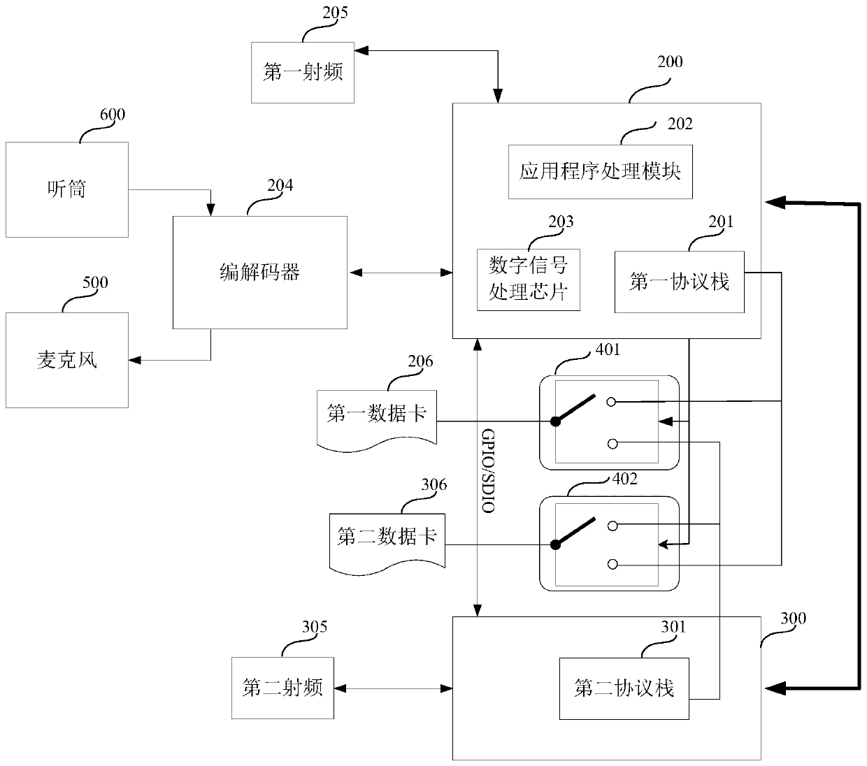
[0054] see figure 2 It is a schematic structural diagram of a user equipment according to an embodiment of the present invention. The user equipment 100 in the embodiment of the present invention performs wireless communication based on Long Term Evolution (LTE), and it can support dual LTE. specific:
[0055] see figure 2 , the user equipment in one embodiment of the present invention includes: a first processing chip 200, a second processing chip 300, a first radio frequency 205, a second radio frequency 305, a first data card 206, a second data card 306, a codec 204, A first logic switch 401 , a second logic switch 402 , an earpiece 600 , and a microphone 500 . Wherein, the first processing chip 200 includes an application program processing module 202 , a digital signal processing chip 203 and a first protocol stack 201 . The second processing chip includes a second protocol stack 301 .
[0056] It should be understood that the digital signal processing chip 203 may...
Embodiment 2
[0129] see Figure 6 On the basis of the first embodiment above, the first processing chip 200 at least includes the following pins: power supply pin (VSIM pin), reset pin (RST pin), clock pin (CLK pin), data pin Pin (DATA pin), first switch control pin (SW1), detection pin (DET), second switch control pin (SW2), multiple input and output pins (UART_GPIO, GPIO, USB_HS, etc.).
[0130] The second processing chip 300 includes at least the following pins: power supply pin (VSIM pin), reset pin (RST pin), clock pin (CLK pin), data pin (DATA pin), detection pin (DET), multiple input and output pins (UART_GPIO, GPIO, USB_HS, etc.).
[0131] The first logic switch 401 is used to connect the power supply pin (VSIM pin) of the first processing chip 200 and the Vcc pin of the first data card 206 under the control of the first switch control pin (SW1). The reset pin (RST pin) of the first processing chip 200 is connected to the RESET pin of the first data card 206, and the clock pin (C...
Embodiment 3
[0141] see Figure 7 On the basis of the first embodiment above, in this embodiment, the first processing chip 200 controls the first logic switch 401 so that the first data card 206 is connected to the first protocol stack 201 . The first processing chip 200 controls the second logic switch 402 so that the second data card 306 is connected to the second protocol stack 301 .
[0142] Therefore, in this embodiment, the first data card 206 resides in the PS domain of the 4G network through the first protocol stack 201, and performs PS data services through the 4G network, and the second data card 306 resides in the PS domain through the second protocol stack 301. In the PS domain of the 4G network, the PS data service is performed through the 4G network.
[0143] The first protocol stack 201 supports the LTE protocol, and the second protocol stack 301 also supports the LTE protocol. When the data service is to be transmitted, the data service transmission can be performed thro...
PUM
 Abstract
Description
Claims
Application Information


