Organic light-emitting diode display substrate, manufacturing method therefore, and display device thereof

A technology for light-emitting diodes and display substrates, which is used in semiconductor/solid-state device manufacturing, electrical components, and electrical solid-state devices, etc., and can solve problems such as large climbing distances for organic thin films.

Inactive Publication Date: 2016-08-31
BOE TECH GRP CO LTD
View PDF6 Cites 52 Cited by
  • Summary
  • Abstract
  • Description
  • Claims
  • Application Information

AI Technical Summary

Problems solved by technology

[0006] In view of this, the present invention provides an organic light emitting diode display substrate, a manufacturing method thereof, and a display device, which are us

Method used


Image

  • Organic light-emitting diode display substrate, manufacturing method therefore, and display device thereof
  • Organic light-emitting diode display substrate, manufacturing method therefore, and display device thereof
  • Organic light-emitting diode display substrate, manufacturing method therefore, and display device thereof

Examples


Embodiment Construction

[0041] The specific implementation manner of the present invention will be further described in detail below with reference to the drawings and embodiments. The following examples are used to illustrate the present invention, but are not intended to limit the scope of the present invention.

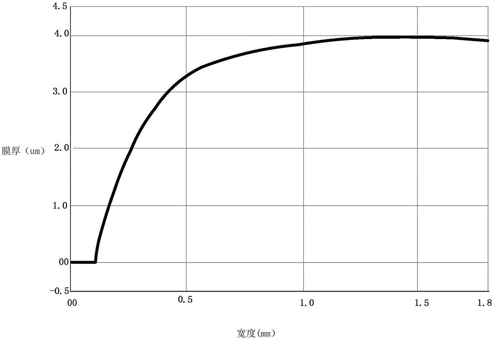
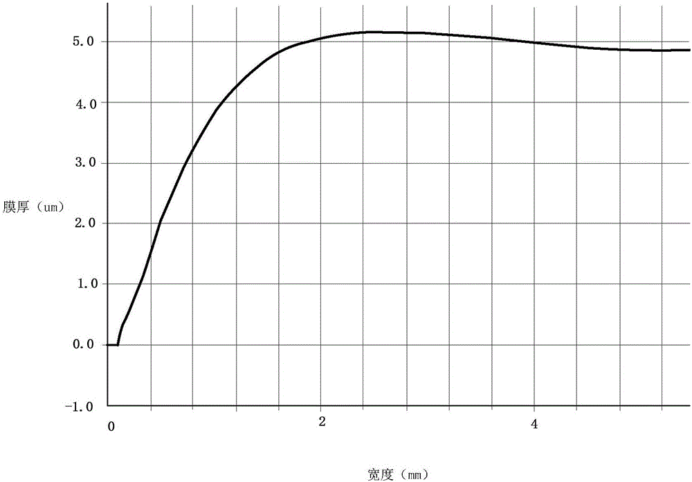
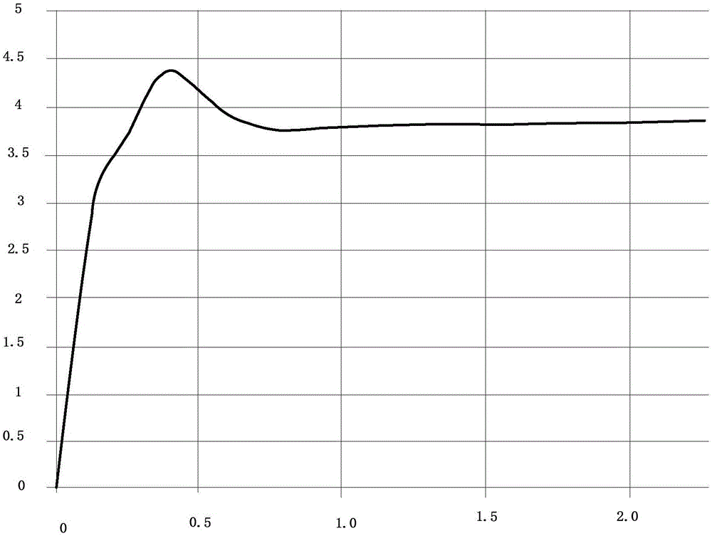
[0042] Please refer to Figure 4 , Figure 4 It is a cross-sectional view of an organic light emitting diode display substrate according to Embodiment 1 of the present invention. The organic light emitting diode display substrate according to this embodiment of the present invention includes: a base substrate 401, an organic light emitting diode device 402 disposed on the base substrate 401, and a thin film package A layer 403 and a hydrophobic barrier 404, the thin film encapsulation layer 403 is used to encapsulate the organic light emitting diode device 402, and includes an inorganic thin film layer 4031 and an organic thin film layer 4032 arranged alternately. The hydrophobic barrie...


PUM

PropertyMeasurementUnit
Widthaaaaaaaaaa
Thicknessaaaaaaaaaa
Widthaaaaaaaaaa

Abstract

The present invention provides an organic light-emitting diode display substrate, a manufacturing method therefore, and a display device thereof. The organic light-emitting diode display substrate comprises a substrate, an organic light-emitting diode device located on the substrate and a film encapsulation layer. The film encapsulation layer is configured to package the organic light-emitting diode device, and includes at least one inorganic thin layer and at least one organic thin layer which are mutually and alternatively arranged and a hydrophobic retaining wall with a micro-nano structure arranged on the substrate and located at the periphery of the film encapsulation layer. The hydrophobic retaining wall is formed prior to formation of the organic thin layer, and is able to block the fluidity of the ink used for ink-jet printing when a printing technology is employed to prepare the organic thin layer so as to restrict the climbing distance of the organic thin layer and provide technology guarantee for the narrow-edge framing of displaying products of a soft organic light-emitting diode.

Description

technical field [0001] The invention relates to the field of display technology, in particular to an organic light emitting diode display substrate, a manufacturing method thereof, and a display device. Background technique [0002] Encapsulation technology is a key technology for organic light-emitting diode (OLED) display products. Currently, almost all display panel manufacturers are developing thin film encapsulation (TFE). The thin-film packaging structure is generally a multi-layer thin-film stack structure of two or more layers, which can be divided into two types: inorganic thin-film layers and organic thin-film layers according to their functions. [0003] The main function of the inorganic thin film layer is to block water and oxygen, and the main function of the organic thin film layer is to provide planarized film deposition conditions for the subsequently formed inorganic thin film layer and provide excellent particle coating effect. The formation methods of or...

Claims


Application Information

Patent Timeline
IPC IPC(8): H01L27/32H01L51/52H01L51/56
CPCH10K59/12H10K50/8426H10K71/00
Inventor 黄维
Owner BOE TECH GRP CO LTD
Why Eureka
Try Eureka