Manufacturing method of flexible AMOLED (active matrix/organic light emitting diode) display screen and conductive adhesive film layer

A technology of conductive adhesive film and production method, which is applied in semiconductor/solid-state device manufacturing, circuit, photovoltaic power generation, etc., can solve problems such as cracks on flexible substrates, failure of conduction between IC chips and bonding terminals, etc., to avoid crack defects, The effect of simple preparation process

Active Publication Date: 2017-06-13
WUHAN CHINA STAR OPTOELECTRONICS TECH CO LTD
View PDF4 Cites 17 Cited by
  • Summary
  • Abstract
  • Description
  • Claims
  • Application Information

AI Technical Summary

Problems solved by technology

[0007] The purpose of the present invention is to provide a kind of flexible AMOLED display screen, can avoid the crack defect that occurs in the flexible substrate in the bonding process as in the prior art, and the IC chip and the bonding terminal cannot be connected because the conductive particles are not broken. common problem
[0008] The purpose of the present invention is also to provide a method for making a conductive adhesive film layer, which can be applied to a flexible AMOLED display to avoid the occurrence of a flexible substrate in the bonding process as in the prior art Crack defects, and the problem that the IC chip and the bonding terminal cannot be conducted due to the unruptured conductive particles

Method used


Image

  • Manufacturing method of flexible AMOLED (active matrix/organic light emitting diode) display screen and conductive adhesive film layer
  • Manufacturing method of flexible AMOLED (active matrix/organic light emitting diode) display screen and conductive adhesive film layer
  • Manufacturing method of flexible AMOLED (active matrix/organic light emitting diode) display screen and conductive adhesive film layer

Examples


Embodiment Construction

[0038] In order to further illustrate the technical means adopted by the present invention and its effects, the following describes in detail in conjunction with preferred embodiments of the present invention and accompanying drawings.

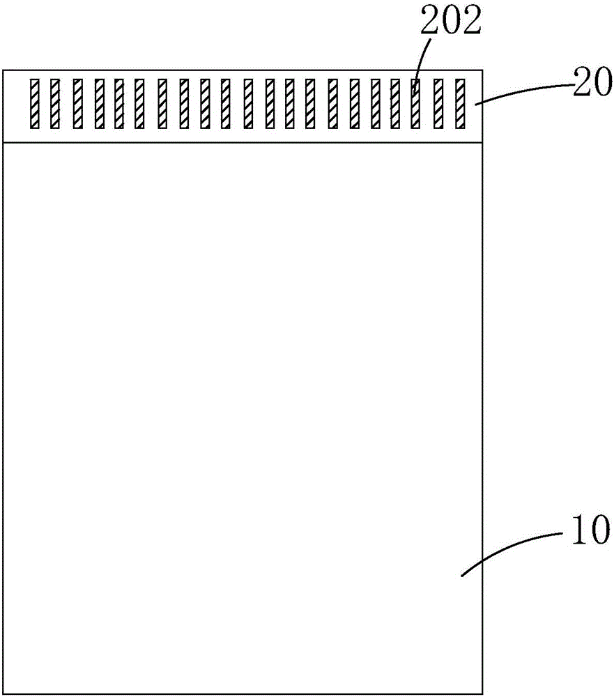
[0039] Please also see Figure 4 and Figure 5 Firstly, the present invention provides a flexible AMOLED display, including a display area 1 and the IC bonding area 2 located on one side of the display area 1 .

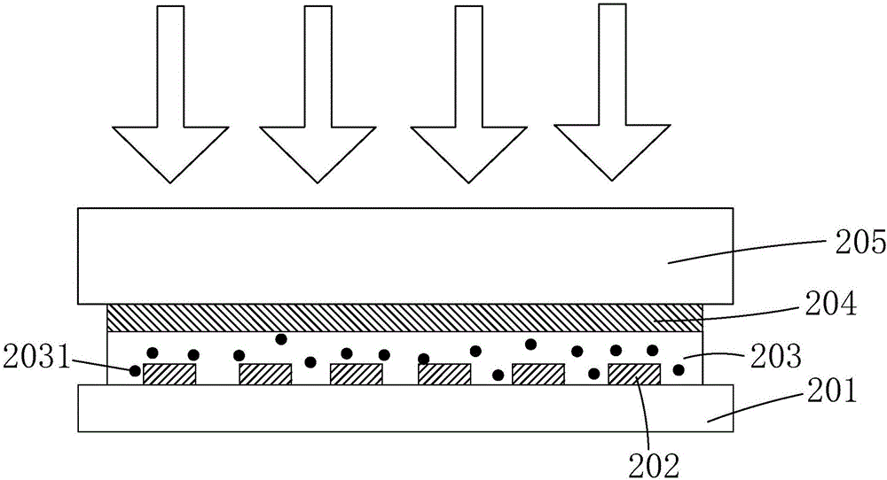
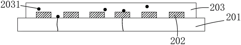
[0040] The IC bonding area 2 is provided with a flexible substrate 21, a plurality of bonding terminals 22 disposed on the flexible substrate 21, disposed on the flexible substrate 21 and covering the plurality of bonding terminals 22, the conductive adhesive film layer 23, and the IC chip 24 disposed on the conductive adhesive film layer 23.

[0041] The conductive adhesive film layer 23 is different from the existing anisotropic conductive adhesive film, does not contain conductive particles, but includes a multi-layer conductive fi...


PUM


Abstract

The invention provides a manufacturing method of a flexible AMOLED (active matrix/organic light emitting diode) display screen and a conductive adhesive film layer. The flexible AMOLED display screen is provided with a flexible substrate (21), a plurality of bonding terminals (22), a conductive adhesive film layer (23) and an IC (integrated circuit) chip by layers from bottom to top; the conductive adhesive film layer (23) comprises a plurality of conductive thin films (231) and a plurality of insulation thin films (232), which are sequentially and alternatively staggered in the extending direction of the IC chip (24); the conductive thin films (231) are used for replacing the conductive particles which are dispersed in the existing anisotropic conductive adhesive thin films and only can be broken by larger stress to conduct the IC chip (24) and the bonding terminals (22). The manufacturing method can solve the problems of cracks of the flexible substrate and failure to conduct the IC chip and the bonding terminal due to the unbroken conductive particles in the bonding process of the prior art.

Description

technical field [0001] The invention relates to the field of display technology, in particular to a method for manufacturing a flexible AMOLED display screen and a conductive adhesive film layer. Background technique [0002] In the field of display technology, organic light emitting diode display (Organic Light Emitting Diode, OLED) has thin, light, wide viewing angle, active light emission, continuously adjustable light color, low cost, fast response speed, low energy consumption, low driving voltage, Wide operating temperature range, simple production process, high luminous efficiency and flexible display, etc., are known as "dream display". According to the driving method, OLED screens can be divided into two categories: Passive Matrix (PM) OLED and Active Matrix (AM) OLED, namely direct addressing and thin film transistor (Thin Film Transistor, TFT) matrix. Two classes of addressing. [0003] In the production process of flexible (Flexible) AMOLED displays, Anisotropi...

Claims


Application Information

Patent Timeline
Patent Type & Authority Applications(China)
IPC IPC(8): H01L51/50H01L51/52H01L51/56H01L51/00H01L27/32
CPCH10K59/12H10K77/111H10K50/00H10K50/80H10K71/00Y02E10/549Y02P70/50
Inventor 刘典
Owner WUHAN CHINA STAR OPTOELECTRONICS TECH CO LTD
Why Eureka
Try Eureka