Check patentability & draft patents in minutes with Patsnap Eureka AI!

Method and device for spi to automatically adjust sampling phase

A sampling phase and automatic adjustment technology, applied in special data processing applications, instruments, electrical digital data processing, etc., can solve the problems of waste of material resources and human resources, incorrect clock and data phase, and can not be done, so as to reduce Effects of manpower and material resources, reduction of design difficulty, and improvement of robustness

Active Publication Date: 2018-08-07
FUZHOU ROCKCHIP SEMICON
View PDF5 Cites 0 Cited by
  • Summary
  • Abstract
  • Description
  • Claims
  • Application Information

AI Technical Summary

Problems solved by technology

[0003] SPI is a commonly used data communication interface at present, and is widely used in the communication between various chips. However, due to the high transmission speed of SPI, and the data receiving end needs to use the received clock to sample the received data, so this has great influence on PCB layout. The board has very high requirements, and it is necessary to pay great attention to the trace length of the clock and data wires, otherwise it is easy to cause the phase of the clock and data sent by the sending end to be incorrect, but when it reaches the receiving end after the PCB trace delay, the receiving clock The phase change with the received data does not meet the sampling timing requirements, which eventually leads to wrong sampling. At the same time, because the SPI output phases of different chips are different, different PCB traces need to be designed for the SPI interface of different chips, which cannot be done on one circuit board. Universal adaptation of SPI for different chips, resulting in a great waste of material and human resources
[0004] That is to say, in the current SPI design of the chip, the output phase of the SPI interface is fixed, so there are very high requirements for the PCB layout, and it is necessary to pay great attention to the length of the clock and data wires, otherwise it is easy to cause the sender The phases of the clock and data sent out are incorrect, but when they arrive at the receiving end after the delay of the PCB trace, the phase of the receiving clock and the received data changes and does not meet the sampling timing requirements, eventually resulting in wrong sampling
Moreover, since the SPI output phases of different chips are different, different PCB traces need to be designed for the SPI interfaces of different chips, and it is impossible to make one circuit board universally adaptable to the SPI of different chips, resulting in a lot of material and human resources. waste

Method used


Image

  • Method and device for spi to automatically adjust sampling phase

Examples


Embodiment Construction

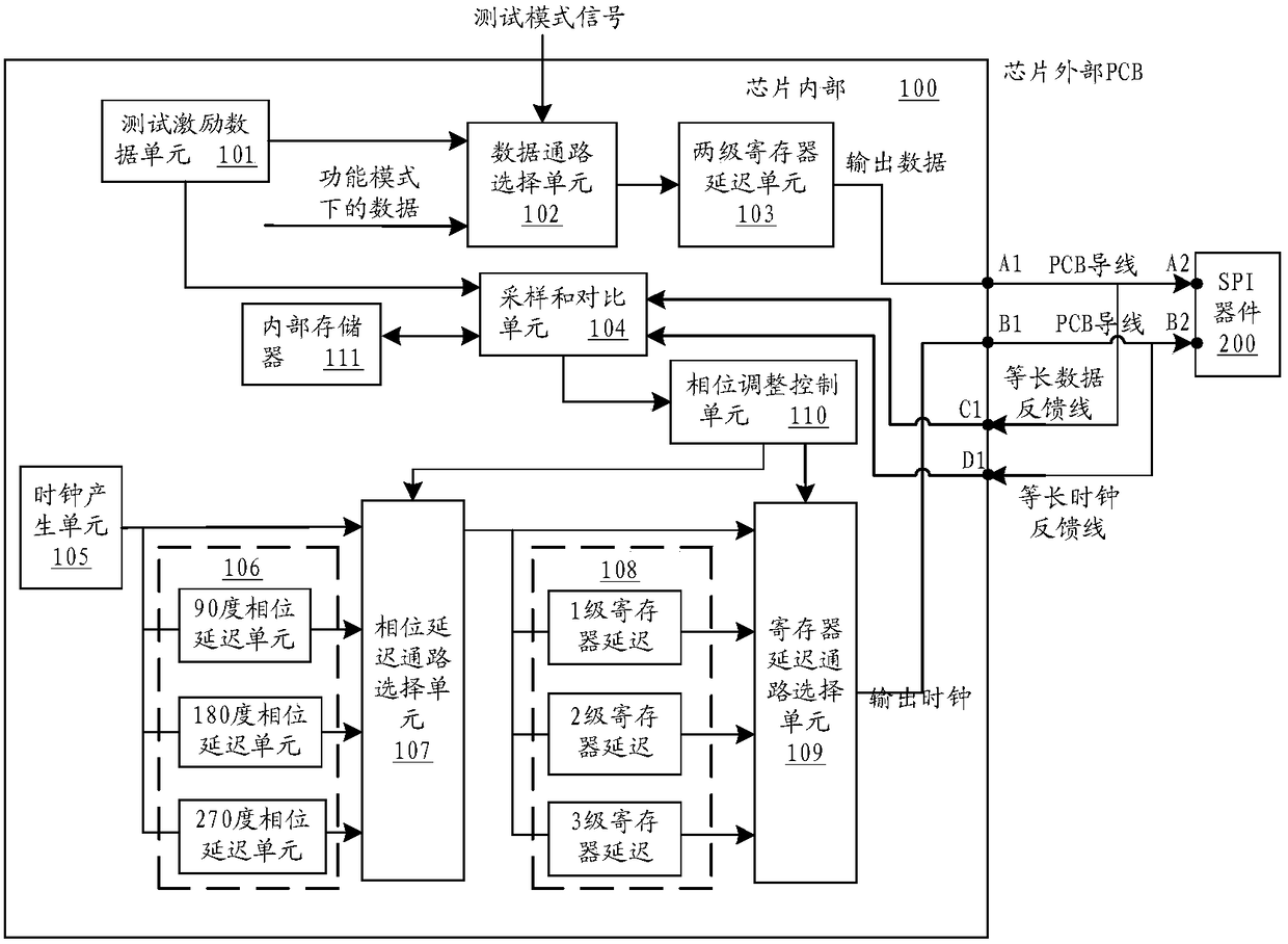
[0055] The method for SPI automatic adjustment sampling phase of the present invention comprises:

[0056] (1) Carry out adaptive training on the PCB board before the first normal working mode, and first control the test mode signal to be valid;

[0057] (2) The test stimulus data is strobed and sent out according to the transmission clock frequency of the pre-stored data sequence, and sent to the data pin port of the main control chip after being delayed by two-stage registers, and then transmitted to the data of the SPI device through the PCB wire pin feet; at the same time

[0058] The data transmission clock of the SPI device is output to the clock pin port of the main control chip after phase delay and register delay in sequence, and then transmitted to the clock pin of the SPI device through the PCB wire;

[0059] (3) by controlling the phase delay and the register delay, until the internal phase delay configuration of the chip that best matches the PCB board phase dela...


PUM


Abstract

The invention provides a method and a device for a SPI (Serial Peripheral Interface) to automatically regulating a sampling phase position. The method comprises the following steps: before a normal work mode is carried out for the first time, adaptive training is carried out on a PCB (Printed Circuit Board), test incentive data is subjected to gating during testing and is transmitted according to the transmission clock frequency of a pre-stored data series, the test incentive data is sent to the data pin port of a main control chip after the test incentive data is delayed by two stages of registers, and then, the test incentive data is transmitted to the data pin of a SPI device through a PCB lead; meanwhile, the data transmission clock of the SPI is output to the clock pin port of the main control chip successively through phase position delay and register delay, and is transmitted to the clock pin of the SPI device via the PCB lead; and the phase position delay and the register delay are controlled until a chip internal phase delay configuration which is optimally matched with the PCB-stage phase delay for the main control chip to use during normal work. The method and the device can achieve optimal clock phase position adaptability under a default situation, can carry out adaptive regulation by aiming at different external circuit boards, and can achieve the optimal matching effect with different PCB electrical conditions.

Description

technical field [0001] The invention relates to a design of an SPI clock, in particular to a method and a device for automatically adjusting the sampling phase of the SPI. Background technique [0002] SPI (Serial Peripheral Interface, Serial Peripheral Interface) is a high-speed, full-duplex, synchronous communication bus, and only occupies four wires on the pins of the chip, which saves the pins of the chip and provides PCB The layout saves space and provides convenience. It is because of this easy-to-use feature that more and more chips integrate this communication protocol. [0003] SPI is a commonly used data communication interface at present, and is widely used in the communication between various chips. However, due to the high transmission speed of SPI, and the data receiving end needs to use the received clock to sample the received data, so this has great influence on PCB layout. The board has very high requirements, and it is necessary to pay great attention to ...

Claims


Application Information

Patent Timeline
Patent Type & Authority Patents(China)
IPC IPC(8): G06F17/50
CPCG06F30/398
Inventor 廖裕民吴占敏
Owner FUZHOU ROCKCHIP SEMICON
Features
  • R&D
  • Intellectual Property
  • Life Sciences
  • Materials
  • Tech Scout
  • Unparalleled Data Quality
  • Higher Quality Content
  • 60% Fewer Hallucinations
Learn More