Check patentability & draft patents in minutes with Patsnap Eureka AI!

Adaptive adjustment method and device for I2S peripheral circuit timing sequence

A technology of self-adaptive adjustment and peripheral circuits, which is used in electrical digital data processing, instruments, etc., to achieve the effects of high adjustment accuracy, reduced design difficulty, and improved robustness

Active Publication Date: 2016-09-21
FUZHOU ROCKCHIP SEMICON
View PDF5 Cites 3 Cited by
  • Summary
  • Abstract
  • Description
  • Claims
  • Application Information

AI Technical Summary

Problems solved by technology

However, there is currently no publicity of relevant information that can solve this technical problem.

Method used


Image

  • Adaptive adjustment method and device for I2S peripheral circuit timing sequence
  • Adaptive adjustment method and device for I2S peripheral circuit timing sequence

Examples


Embodiment Construction

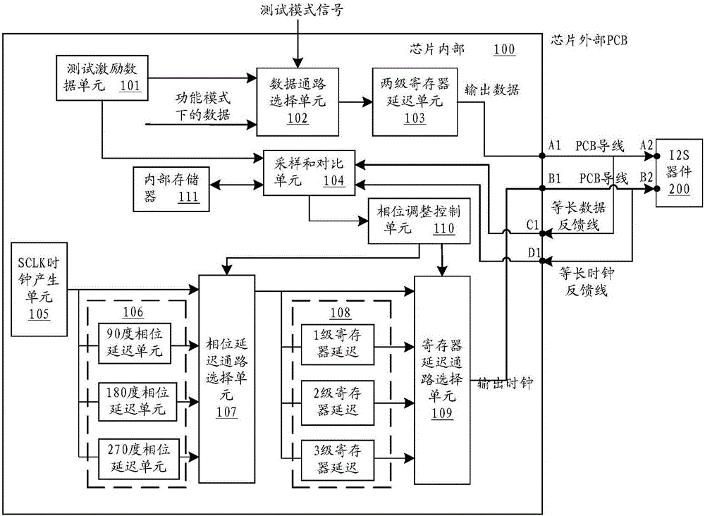
[0065] Such as figure 2 As shown, the adaptive adjustment method of I2S peripheral circuit timing of the present invention comprises the following steps:

[0066] (1) Adaptive training of the PCB board before the first normal working mode, first control the test mode signal to be set to be valid;

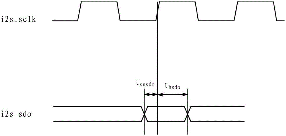
[0067] (2) The test stimulus data is strobed and sent out according to the transmission clock frequency of the pre-stored data sequence, and sent to the data pin port of the main control chip after being delayed by two-stage registers. Then it is transmitted to the data pin of the I2S device through the PCB wire feet; at the same time

[0068] The I2S data transmission clock is output to the clock pin port of the main control chip after phase delay and register delay in sequence, and then transmitted to the clock pin pin of the I2S device through the PCB wire;

[0069] (3) by controlling the phase delay and the register delay, until the internal phase delay configuration of the c...


PUM


Abstract

The invention provides an adaptive adjustment method and device for an I2S peripheral circuit timing sequence. The method comprises the following steps: carrying out adaptive training on a PCB before a first time normal working mode, and controlling to set a test mode signal as effective at first; gating test incentive data, outputting the test incentive data according to pre-stored transmission clock frequency of a data sequence, outputting the test incentive data to a data pin port of a main control chip after the delay of two levels of registers, and then transmitting the test incentive data to a data pin of an I2S device through a PCB conducting wire; meanwhile, outputting the data transmission clock of I2S to the clock pin port of the main control chip after phase delay and register delay in sequence, and then transmitting the data transmission clock to the clock pin of the I2S device through the PCB conducting wire; and controlling the phase delay and the register delay until finding the optimal delay configuration that is optimally matched with the PCB for the normal work of the main control chip. The optimal clock phase adaptability can be achieved in default, and different external circuit boards can be adaptively adjusted to achieve optimal matching effects with different PCB electrical conditions.

Description

technical field [0001] The invention relates to a chip technology, in particular to a method and device for self-adaptive adjustment of timing sequence of an I2S peripheral circuit of a chip. Background technique [0002] The I2S (Inter-IC Sound) bus, also known as the integrated circuit built-in audio bus, is a bus standard developed by Philips for audio data transmission between digital audio devices. The bus is dedicated to data transmission between audio devices. Widely used in various multimedia systems. It adopts the design of transmitting clock and data signals along independent wires. By separating the data and clock signals, it avoids the distortion induced by time difference and saves the cost of purchasing professional equipment against audio jitter for users. [0003] I2S is a commonly used data communication interface at present, and is widely used in the communication between various chips. However, due to the high transmission speed of I2S, and at the same ti...

Claims


Application Information

Patent Timeline
IPC IPC(8): G06F13/372G06F13/42
CPCG06F13/372G06F13/4282G06F2213/0016
Inventor 廖裕民
Owner FUZHOU ROCKCHIP SEMICON
Features
  • R&D
  • Intellectual Property
  • Life Sciences
  • Materials
  • Tech Scout
  • Unparalleled Data Quality
  • Higher Quality Content
  • 60% Fewer Hallucinations
Learn More