Integrated use of model-based metrology and a process model

a technology of process model and metrology, applied in the field of metalrology system and method, can solve the problems of difficult characterization, difficult penetration of optical radiation to the bottom layer, and difficulty in characterization, so as to improve the prediction results of one or both of the metrology model and the process model

a technology of process model and metrology, applied in the field of metalrology system and method, can solve the problems of difficult characterization, difficult penetration of optical radiation to the bottom layer, and difficulty in characterization, so as to improve the prediction results of one or both of the metrology model and the process model

US20140172394A1Active Publication Date: 2014-06-19KLA TENCOR TECH CORP

Image

  • Integrated use of model-based metrology and a process model
  • Integrated use of model-based metrology and a process model
  • Integrated use of model-based metrology and a process model

Examples


Embodiment Construction

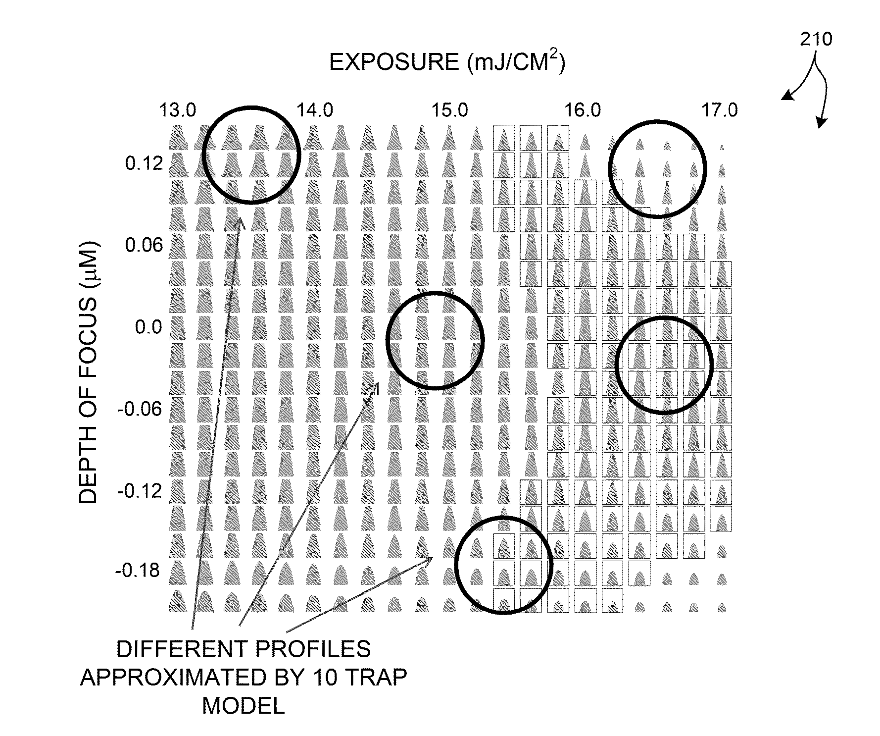
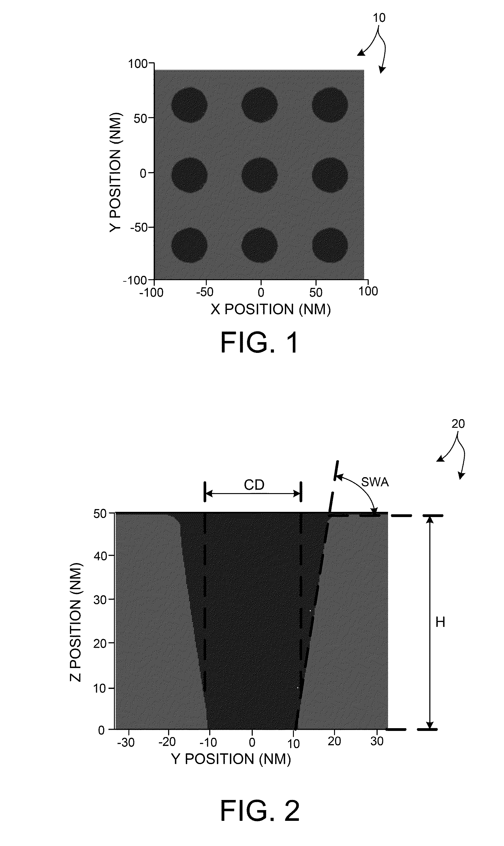
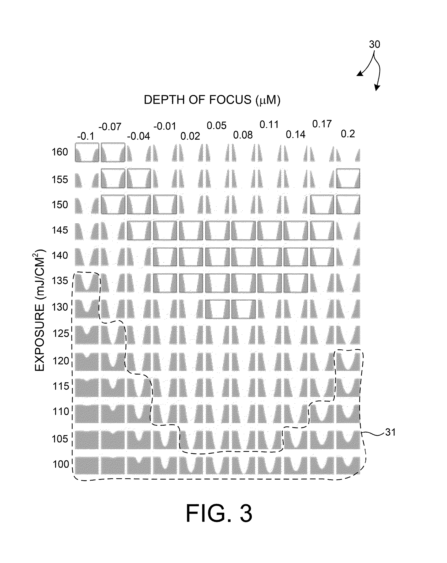
[0044]Reference will now be made in detail to background examples and some embodiments of the invention, examples of which are illustrated in the accompanying drawings. Methods and systems for optimizing measurement models based on integrating a process-based target model with a metrology-based target model are presented. By integrating a metrology based target model with process based target model, the predictive results of one or both of the metrology model and the process model are improved.

[0045]In general, optical metrology techniques are indirect methods of measuring physical properties of a specimen under inspection. In most cases, the measured optical signals cannot be used to directly determine the physical properties of interest. Traditionally, the measurement process consists of formulating a metrology model that attempts to predict the measured optical signals based on a model of the interaction of the measurement target with the particular metrology system. The metrolog...


PUM


Abstract

Methods and systems for performing measurements based on a measurement model integrating a metrology-based target model with a process-based target model. Systems employing integrated measurement models may be used to measure structural and material characteristics of one or more targets and may also be used to measure process parameter values. A process-based target model may be integrated with a metrology-based target model in a number of different ways. In some examples, constraints on ranges of values of metrology model parameters are determined based on the process-based target model. In some other examples, the integrated measurement model includes the metrology-based target model constrained by the process-based target model. In some other examples, one or more metrology model parameters are expressed in terms of other metrology model parameters based on the process model. In some other examples, process parameters are substituted into the metrology model.

Description

CROSS REFERENCE TO RELATED APPLICATION[0001]The present application for patent claims priority under 35 U.S.C. §119 from U.S. provisional patent application Ser. No. 61 / 738,760, entitled “Method for Integrated Use of Model-based Metrology and a Process Model,” filed Dec. 18, 2012, the subject matter of which is incorporated herein by reference in its entirety.TECHNICAL FIELD[0002]The described embodiments relate to metrology systems and methods, and more particularly to methods and systems for improved parameter measurement.BACKGROUND INFORMATION[0003]Semiconductor devices such as logic and memory devices are typically fabricated by a sequence of processing steps applied to a specimen. The various features and multiple structural levels of the semiconductor devices are formed by these processing steps. For example, lithography among others is one semiconductor fabrication process that involves generating a pattern on a semiconductor wafer. Additional examples of semiconductor fabric...

Claims


Application Information

Patent Timeline
19 Jun 2014
Publication
US20140172394A1
IPC
G06F17/50
CPC
G06F17/5009; G03F7/70625; G03F7/70641; G06F30/20; G06F30/398
Inventors
KUZNETSOV, ALEXANDER; SHCHEGROV, ANDREI V.