Check patentability & draft patents in minutes with Patsnap Eureka AI!

Method and apparatus for adjusting phases of EMMC interface and NAND interface

A phase adjustment and interface technology, applied in the field of phase adaptive adjustment, can solve problems such as waste of material resources and human resources, general adaptation of circuit boards to nand flash memory, and wrong sampling, so as to reduce manpower and material resources, reduce design difficulty, and adjust high precision effect

Active Publication Date: 2016-09-07
FUZHOU ROCKCHIP SEMICON
View PDF7 Cites 15 Cited by
  • Summary
  • Abstract
  • Description
  • Claims
  • Application Information

AI Technical Summary

Problems solved by technology

However, due to the high transmission speed of the nand flash memory interface, and at the same time, the data receiving end needs to use the received clock to sample the received data, so this has high requirements for the PCB layout, and it is necessary to pay great attention to the trace length of the clock and data wires , otherwise it is easy to cause the clock and data phases sent by the sending end to be correct, but when they arrive at the receiving end after being delayed by PCB traces, the phases of the receiving clock and received data change and do not meet the sampling timing requirements, eventually resulting in wrong sampling
At the same time, due to the different output phases of the nand flash interface of different chips, different PCB routing needs to be designed for the nand flash interface of different chips, and it is impossible to make one circuit board universally adaptable to the nand flash memory of different chips, resulting in a large material resource and waste of human resources

Method used


Image

  • Method and apparatus for adjusting phases of EMMC interface and NAND interface
  • Method and apparatus for adjusting phases of EMMC interface and NAND interface
  • Method and apparatus for adjusting phases of EMMC interface and NAND interface

Examples


Embodiment 1

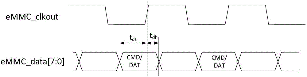
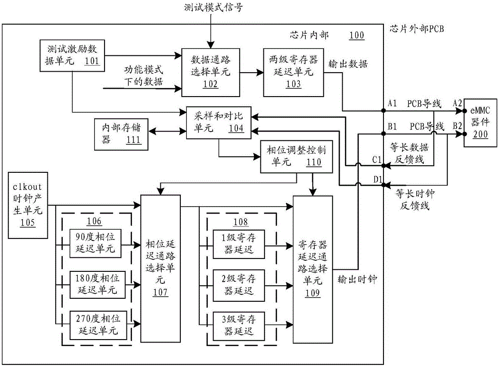
[0041] see image 3 Shown, EMMC interface phase adjustment method of the present invention comprises the following steps:

[0042] (1) Adaptive training of the PCB board before the first normal working mode, first control the test mode signal to be set to be valid;

[0043] (2) The test excitation data is strobed and sent out according to the transmission clock frequency of the pre-stored data sequence, and sent to the data pin port of the main control chip after being delayed by two-stage registers. Then it is transmitted to the data pin of the EMMC device through the PCB wire feet; at the same time

[0044] The data transmission clock of EMMC is output to the clock pin port of the main control chip after phase delay and register delay in sequence, and then transmitted to the clock pin of the EMMC device through the PCB wire;

[0045] (3) by controlling the phase delay and the register delay, until the internal phase delay configuration of the chip that best matches the PCB...

Embodiment 2

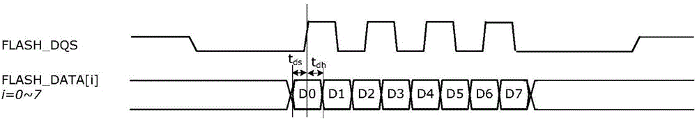
[0092] see Figure 4 Shown, NAND interface phase adjustment method of the present invention comprises the following steps:

[0093] (1) Adaptive training of the PCB board before the first normal working mode, first control the test mode signal to be set to be valid;

[0094] (2) The test stimulus data is strobed and sent out according to the transmission clock frequency of the pre-stored data sequence, and sent to the data pin port of the main control chip after being delayed by two-stage registers. Then the data is transmitted to the NAND flash memory device through the PCB wire pin feet; at the same time

[0095] The data transmission clock of the NAND flash memory is output to the clock pin port of the main control chip after phase delay and register delay in sequence, and then transmitted to the clock pin of the NAND flash memory device through the PCB wire;

[0096] (3) by controlling the phase delay and the register delay, until the internal phase delay configuration o...


PUM


Abstract

The present invention provides a method and an apparatus for adjusting phases of an EMMC interface and a NAND interface. The method comprises that before a first normal operation mode, adaptive training is carried out on a PCB board, and test stimulus data is sent out according pre-stored transmission clock frequency of a data sequence, and after undergoing a two-stage register delay, the data is sent to a data pin port of a master chip, and is transmitted through a PCB wire to a data pin of the EMMC or the NAND device; simultaneously, after sequentially undergoing a phase delay and the two-stage register delay, a data transmission clock of the EMMC or the NAND is output to a clock pin port of the master chip, and is transmitted through the PCB wire to a clock pin of the EMMC or the NAND device; and the phase delay and the two-stage register delay are controlled until a chip exterior phase delay chip configuration optimally matched with the PCB board level phase delay, so as to enable the master chip to carry out EMMC or NAND data transmission during normal operation. Thus, optimal match effects under different PCB electrical conditions can be reached.

Description

technical field [0001] The invention relates to a chip interface technology, in particular to a phase adaptive adjustment method and device for an EMMC chip interface and a NAND flash memory interface. Background technique [0002] EMMC (Embedded Multi Media Card) is an embedded memory standard specification established by the MMC Association, mainly for products such as mobile phones or tablet computers. A clear advantage of eMMC is the integration of a controller in the package, which provides a standard interface and manages the flash memory, freeing handset manufacturers to focus on other parts of product development and reducing time-to-market. [0003] EMMC is a commonly used data communication interface at present, and is widely used in the communication between various chips. However, due to the high transmission speed of EMMC, and the data receiving end needs to use the received clock to sample the received data, so this has a great impact on the PCB layout. The bo...

Claims


Application Information

Patent Timeline
Patent Type & Authority Applications(China)
IPC IPC(8): G06F11/26
CPCG06F11/26
Inventor 廖裕民
Owner FUZHOU ROCKCHIP SEMICON
Features
  • R&D
  • Intellectual Property
  • Life Sciences
  • Materials
  • Tech Scout
  • Unparalleled Data Quality
  • Higher Quality Content
  • 60% Fewer Hallucinations
Learn More