A kind of tapered microwell array and its preparation method
A microhole array, tapered technology, applied in the field of material processing
- Summary
- Abstract
- Description
- Claims
- Application Information
AI Technical Summary
Problems solved by technology
Method used
Image
Examples
Embodiment
[0030] The diamond film is selected as a non-metallic film with a size of 5x5mm and a thickness of 0.2mm; before the non-metallic film is processed, the upper and lower surfaces of the film are ground and polished to make the surface roughness 0.1-1μm, and then soaked in alcohol and ultrasonically cleaned for 20 minutes to remove the attached Impurities and oil stains are then dried to obtain a non-metallic film for use;
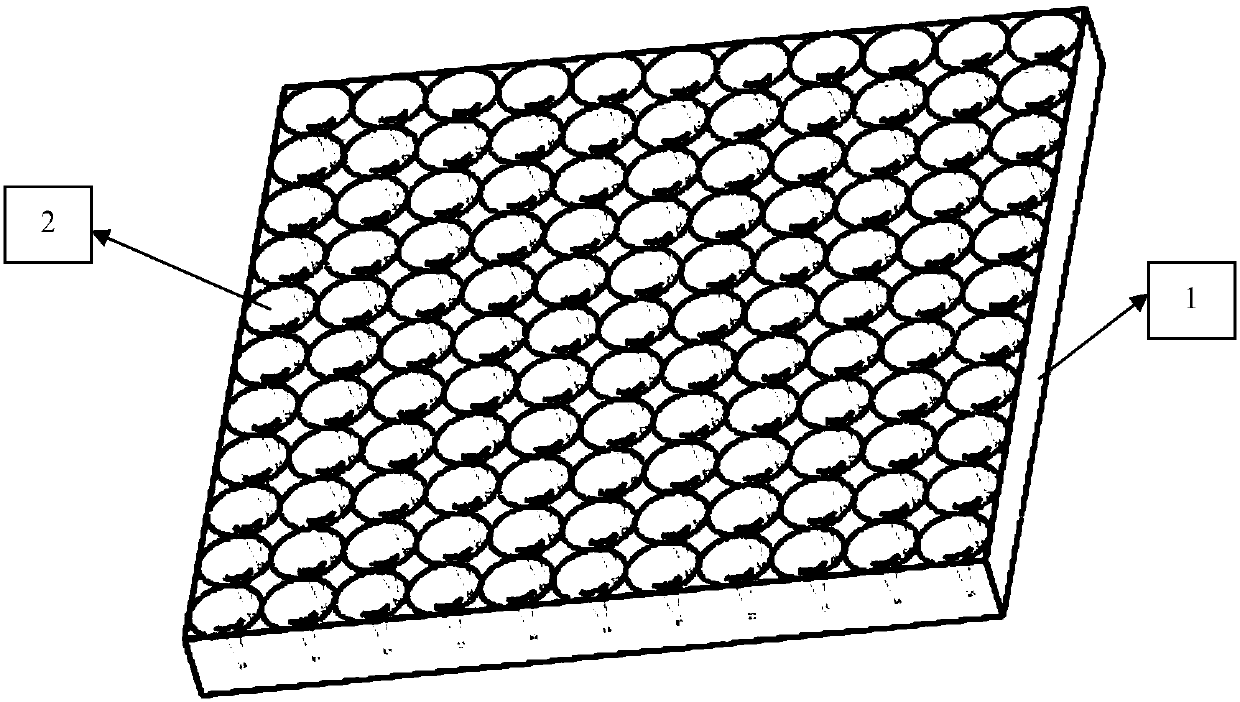
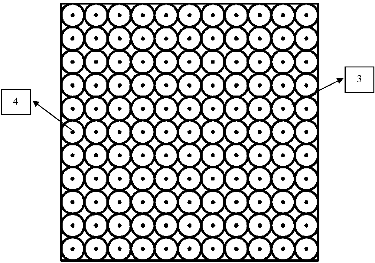
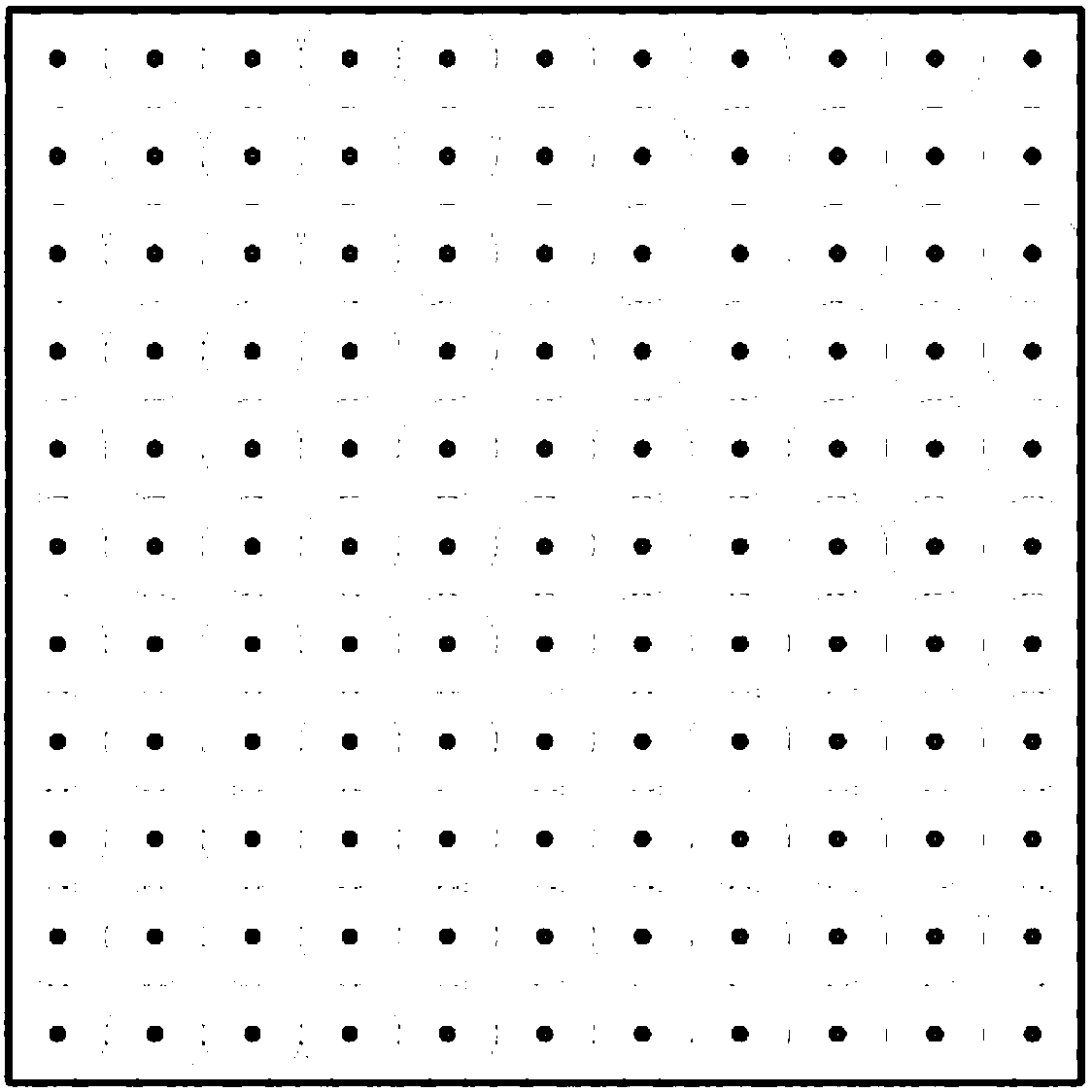
[0031] Create a graphic file of the microwell array, use the graphic design software to design the microwell entrance pattern with an aperture diameter of 20 μm, and a distance between the centerlines of the microholes of 100 μm, turn on the fiber pulse laser (Hantong HT-20F laser equipment), and place the non-metallic film on the working surface. On the stage, adjust the focus of the laser so that the laser focus falls on the surface of the film, import the graphics file, set the wavelength of the fiber pulse laser to 1064nm, the power to 20w, and set the la...
PUM
| Property | Measurement | Unit |
|---|---|---|
| thickness | aaaaa | aaaaa |
| surface roughness | aaaaa | aaaaa |
Abstract
Description
Claims
Application Information


