Display panel with fingerprint identification function, preparation method and display device

A display panel and fingerprint recognition technology, which is applied in semiconductor/solid-state device manufacturing, electrical components, electric solid-state devices, etc., can solve the problems of cost increase and process complexity increase, and achieve the effect of saving cost and reducing process complexity

Active Publication Date: 2016-10-12
BOE TECH GRP CO LTD
View PDF4 Cites 48 Cited by
  • Summary
  • Abstract
  • Description
  • Claims
  • Application Information

AI Technical Summary

Problems solved by technology

Therefore, it is necessary to develop an OLED display with a fingerprint recognition function, but integrating the mutual-capacity fi

Method used


Image

  • Display panel with fingerprint identification function, preparation method and display device
  • Display panel with fingerprint identification function, preparation method and display device
  • Display panel with fingerprint identification function, preparation method and display device

Examples


Embodiment Construction

[0060] Embodiments of the present application provide a display panel with a fingerprint recognition function, a manufacturing method, and a display device, so as to realize an OLED display with a fingerprint recognition function, reduce process complexity, and save costs.

[0061] The following will clearly and completely describe the technical solutions in the embodiments of the application with reference to the drawings in the embodiments of the application. Apparently, the described embodiments are only some of the embodiments of the application, not all of them. Based on the embodiments in this application, all other embodiments obtained by persons of ordinary skill in the art without making creative efforts belong to the scope of protection of this application.

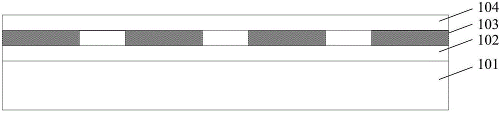
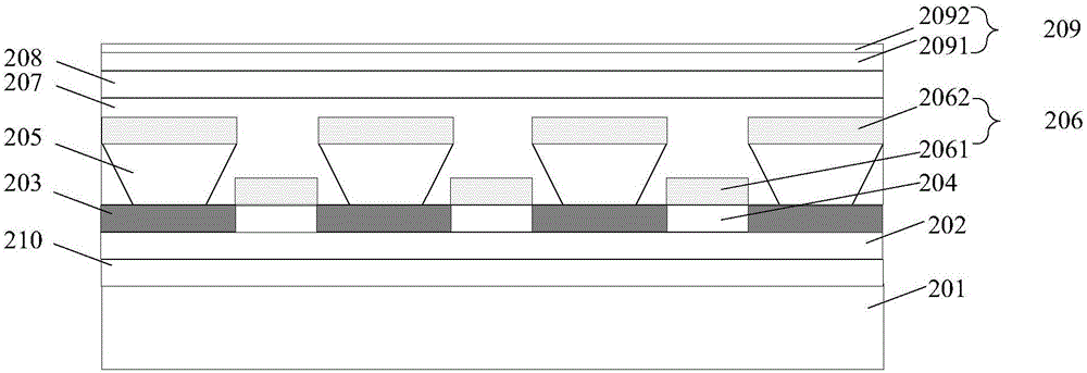
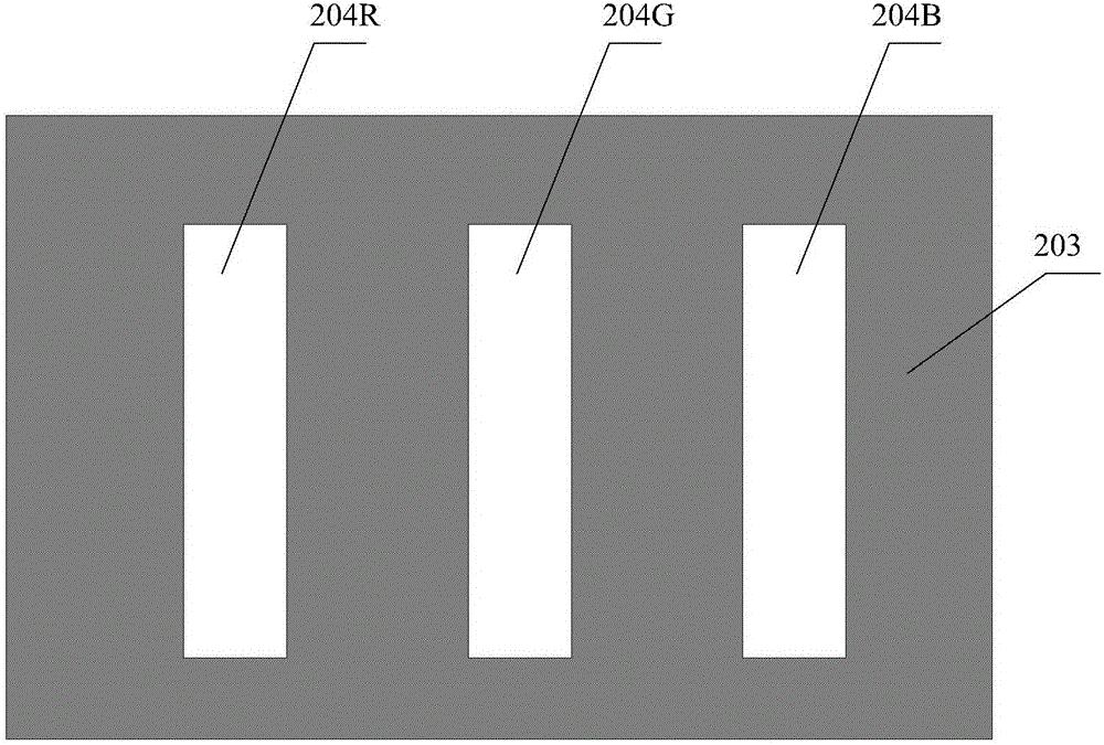
[0062] It should be noted that the thickness and shape of each layer in the drawings of the present application do not reflect the real scale, and the purpose is only to schematically illustrate the content of th...


PUM


Abstract

The invention provides a display panel with a fingerprint identification function, a preparation method and a display device for achieving an OLED display with the fingerprint identification function, reducing the process complexity and saving the cost. The display panel with the fingerprint identification function provided by the invention comprises an array substrate, an anode layer, a pixel definition region, a plurality of organic light-emitting units, an isolating column, a reuse electrode layer, a second electrode layer and a cover plate, wherein the anode layer is located on the array substrate; the plurality of organic light-emitting units are surrounded by the pixel definition region; the pixel definition region and the organic light-emitting units are located on the anode layer; the isolating column is located on the pixel definition region; the reuse electrode layer is located on the isolating column and the organic light-emitting units; the reuse electrode layer comprises a cathode layer and a first electrode layer; the reuse electrode layer covering the isolating column is taken as a first electrode layer; the reuse electrode layer surrounded by the first electrode layer is taken as the cathode layer; the first electrode layer and the cathode layer are arranged on the same layer and are not connected with each other; the second electrode layer is located on the reuse electrode layer; and the cover plate is located on the second electrode layer.

Description

technical field [0001] The present application relates to the field of display technology, in particular to a display panel with a fingerprint identification function, a preparation method, and a display device. Background technique [0002] An organic light-emitting diode (Organic Light-Emitting Diode, OLED) display is also called an organic electroluminescence display (Organic Electroluminescence Display, OELD). Among various types of flat panel displays, OLED displays have the advantages of wide viewing angle, high brightness, high contrast ratio, low driving voltage and fast response. see figure 1 , the existing OLED display panel includes from bottom to top: an array substrate 101, an anode layer 102, an organic light-emitting layer 103, and a cathode layer 104; wherein, the organic light-emitting layer includes a pixel defining region and a plurality of organic light unit ( figure 1 not marked). [0003] Fingerprint is an invariable feature that is unique and disti...

Claims


Application Information

Patent Timeline
IPC IPC(8): H01L27/32H01L51/52H01L51/56
CPCH10K59/122H10K50/82H10K50/805H10K71/00
Inventor 王海生董学薛海林陈小川丁小梁刘英明许睿杨盛际李昌峰刘伟王鹏鹏
Owner BOE TECH GRP CO LTD
Why Eureka
Try Eureka