Wafer level MMCM (microwave multichip module) packaging structure using photosensitive BCB (benzocyclobutene) as dielectric layer and method

A packaging structure and dielectric layer technology, applied in the direction of electrical components, electrical solid devices, circuits, etc., can solve the problems of not meeting the packaging loss requirements of microwave systems, reduce process complexity, improve performance and reliability, and match thermal expansion coefficients Effect

Active Publication Date: 2011-06-29
SHANGHAI INST OF MICROSYSTEM & INFORMATION TECH CHINESE ACAD OF SCI
View PDF1 Cites 33 Cited by
  • Summary
  • Abstract
  • Description
  • Claims
  • Application Information

AI Technical Summary

Problems solved by technology

At present, the thickness of commonly used BCB is only 1um~10um / layer. To meet the high-frequency application, the thickness of BCB should be more than 15um. However, in the current MCM package that uses BCB as the dielectric layer, the thickness of BCB is often below 15um, which cannot meet the requirements of microwave systems. Package Loss Requirements

Method used


Image

  • Wafer level MMCM (microwave multichip module) packaging structure using photosensitive BCB (benzocyclobutene) as dielectric layer and method
  • Wafer level MMCM (microwave multichip module) packaging structure using photosensitive BCB (benzocyclobutene) as dielectric layer and method
  • Wafer level MMCM (microwave multichip module) packaging structure using photosensitive BCB (benzocyclobutene) as dielectric layer and method

Examples


Embodiment Construction

[0057] Embodiments of the present invention will be further specifically described below with reference to the accompanying drawings in order to fully demonstrate the advantages and positive effects of the present invention. The scope of the present invention is not limited to the following examples.

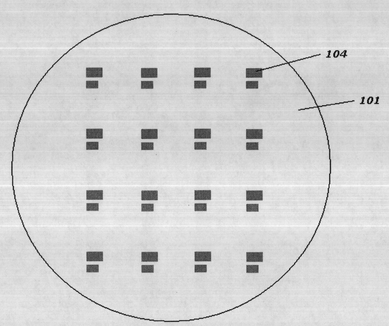
[0058] exist figure 1 Among them, the front side of the silicon substrate 101 is distributed in a 4×4 cell array, and each cell has two cavities of different sizes, which are suitable for embedding chips of different sizes. Since the preparation methods of the two cavities are the same, the larger cavity 104 is taken as an example in the embodiment, and the cavity 104 is formed by wet etching or dry etching.

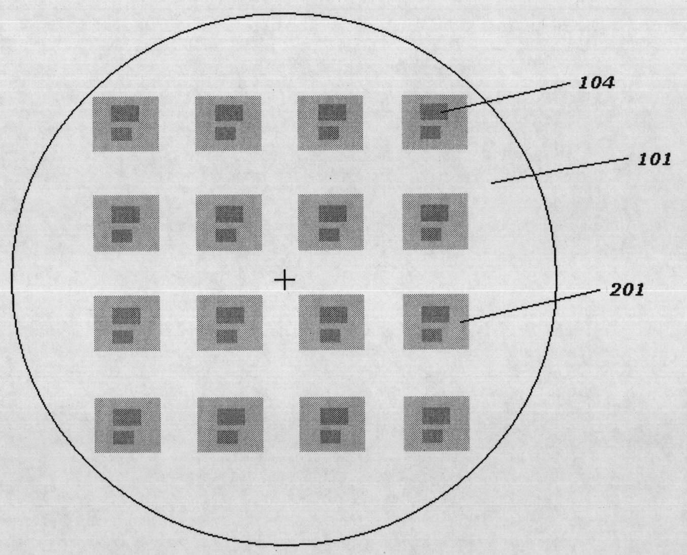
[0059] exist figure 2 In the present invention, the ground shielding layer 201 is prepared on the silicon substrate containing the embedded cavity, and the ground shielding layer 201 is prepared by electroplating.

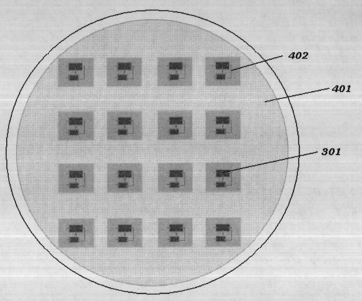
[0060] image 3 It is an overall packaging structure...


PUM


Abstract

The invention relates to a wafer level MMCM (microwave multichip module) packaging structure using photosensitive BCB (benzocyclobutene) as a dielectric layer and a method. The packaging structure is characterized by 1) manufacturing metal ground (GND) shielding layers on a silicon substrate with cavities for embedding; 2) using the photosensitive BCB as the dielectric layers and forming an interconnected through hole structure on the BCB by utilizing photoetching and developing processes; and 3) forming a multi-layer interconnection packaging structure through alternate occurrence of metal layers and the dielectric layers. The method is characterized by eroding or etching the cavities for embedding on the silicon substrate, sputtering a metal seed layer and carrying out electroplating to form the GND, embedding MMIC (monolithic microwave integrated circuit) chips, using conductive adhesives to bond the chips and the substrate, coating the photosensitive BCB and carrying out photoetching and developing to form the interconnected through hole patterns and carrying out curing to realize multi-layer MMCM package. The thickness of the dielectric layers is 20-35mu m. Capacitors, resistors, inductors, power dividers and antenna passive devices can be integrated in the multi-layer interconnection structure or discrete components are integrated through surface mount technology, thus realizing the functionalization of the module.

Description

technical field [0001] The invention relates to a wafer-level MMCM packaging structure and method using a large-thickness photosensitive BCB as a medium layer, and belongs to the field of high-density packaging. Background technique [0002] Microwave Multichip Module (MMCM for short) refers to a multi-chip module used in the high-frequency field, which is developed and matured to meet the miniaturization requirements of phased array radar T / R components. New assembly technology. MCMM directly installs and connects multiple MMIC chips to the substrate substrate. The interconnection distance between the chips is short, which reduces the inductance and impedance of the interconnection line, thus reducing the signal transmission delay time while increasing the assembly density. Improve the transmission speed of the signal, which is conducive to the development of the electronic machine towards functional integration. Compared with the traditional packaging mode, MMCM saves th...

Claims


Application Information

Patent Timeline
Patent Type & Authority Applications(China)
IPC IPC(8): H01L25/00H01L23/31H01L23/522H01L23/528H01L21/50H01L21/768
CPCH01L24/19H01L2224/04105H01L2224/32225H01L2224/73267H01L2224/92244H01L2924/1423H01L2924/15153H01L2924/3025
Inventor 汤佳杰罗乐徐高卫袁媛
Owner SHANGHAI INST OF MICROSYSTEM & INFORMATION TECH CHINESE ACAD OF SCI
Why Eureka
Try Eureka