Graphene high-impedance surface for direction pattern-reconfigurable antenna
A technology of reconstructing antenna and high impedance, applied in the direction of antenna, electrical components, etc., can solve the problems of reducing antenna design cost and control complexity, and achieves regulation of current distribution, maximization of gain, reduction of design cost and subsequent complex reconfiguration. degree of effect
- Summary
- Abstract
- Description
- Claims
- Application Information
AI Technical Summary
Problems solved by technology
Method used
Image

Examples
Embodiment 1
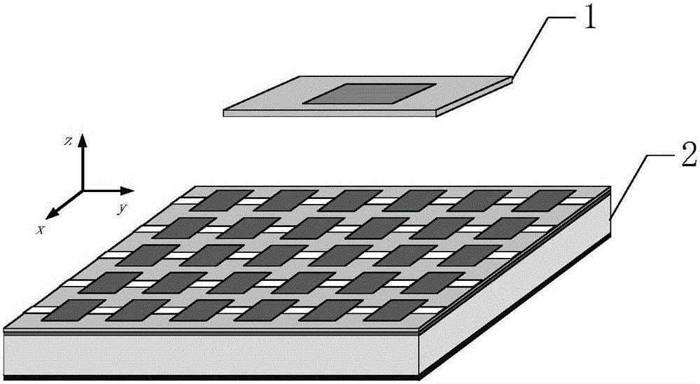
[0025] This embodiment is a theoretical verification example, including the antenna radiation unit 1 and the high-impedance surface 2 .
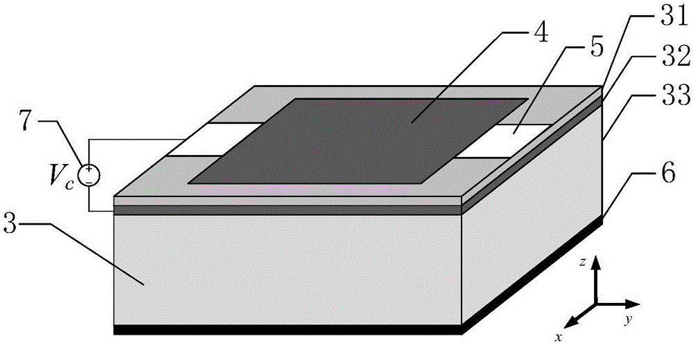
[0026] Figure 2-3 It is a schematic diagram of the structure of a high-impedance surface unit, including a composite dielectric substrate 3, a full metal surface 6 printed on its lower surface, a square metal patch 4 printed in the middle of its upper surface, and graphene connection stickers on the left and right sides of the patch sheet 5, the composite dielectric substrate 3 is composed of an aluminum oxide layer 31, a polysilicon layer 32 and a glass layer 33 stacked sequentially from top to bottom, and a DC bias voltage V is added between the graphene 5 and the polysilicon 32 c 7. It is used to adjust the surface conductivity of the graphene; the aluminum oxide layer 31 in the composite dielectric substrate is used to isolate the polysilicon layer 32 and the graphene 5 to form a bias voltage.
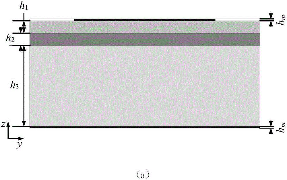
[0027] refer to image 3 , the period o...
Embodiment 2
[0038] Embodiment 2 is an actual reference example, adopting a different form of antenna radiation unit from Embodiment 1, such as Figure 5 As shown in (a), the bottom of the antenna radiation unit is supported by polytetrafluoroethylene 8. At the same time, the polytetrafluoroethylene under the radiator is removed to make it an air cavity. Since the dielectric constant of polytetrafluoroethylene is 2.2, and Below the antenna is an air cavity substrate, which can effectively reduce the back radiation of the antenna. Since the working center frequency f=1.03 THz of the antenna radiation unit selected in this embodiment is the same as that in Embodiment 1, the high-impedance surface unit used is the same.
[0039] refer to Figure 5 , the high-impedance surface 2 in this embodiment is composed of 10×10 high-impedance surface units, and the antenna radiation unit adopts the form of a butterfly antenna, in which the light gray patch is located on the lower surface of the dielect...
PUM
| Property | Measurement | Unit |
|---|---|---|
| thickness | aaaaa | aaaaa |
| thickness | aaaaa | aaaaa |
Abstract
Description
Claims
Application Information
 - R&D Engineer
- R&D Manager
- IP Professional
- Industry Leading Data Capabilities
- Powerful AI technology
- Patent DNA Extraction
Browse by: Latest US Patents, China's latest patents, Technical Efficacy Thesaurus, Application Domain, Technology Topic.
© 2024 PatSnap. All rights reserved.Legal|Privacy policy|Modern Slavery Act Transparency Statement|Sitemap