A kind of dual channel rc-igbt device and preparation method thereof

A dual-channel, device technology, applied in semiconductor/solid-state device manufacturing, semiconductor devices, electrical components, etc., can solve problems such as the path of increasing current, current concentration and uneven temperature, and affect the reliability of RC-IGBT devices. Effects of improving reliability and solving problems of current and temperature uniformity

Active Publication Date: 2019-05-14
UNIV OF ELECTRONICS SCI & TECH OF CHINA
View PDF4 Cites 0 Cited by
  • Summary
  • Abstract
  • Description
  • Claims
  • Application Information

AI Technical Summary

Problems solved by technology

However, this method has the following problems: 1) When the forward IGBT is turned on: due to the existence of parasitic VDMOS, it is difficult to completely eliminate the Snapback phenomenon, and the existence of the N-type collector region 11 makes the turn-on voltage drop of the traditional RC-IGBT larger than that of the traditional IGBT The conduction voltage drop, and the increased width of the P+ collector region will cause the current uniformity of the device when the forward IGBT is turned on, resulting in serious current concentration and temperature unevenness, which seriously affects the reliability of the RC-IGBT device ; 2) When the reverse diode freewheeling conduction: the increased P+ collector area width increases the extraction of the P-type collector area 9 to the holes injected in the N-drift region 7, and increases the path of the current at the same time, increasing the diode The conduction voltage drop, and the increased width of the P+ collector region will cause the current uniformity of the device during the reverse diode freewheeling, resulting in serious current concentration and uneven temperature, which seriously affects the reliability of the RC-IGBT device

Method used


Image

  • A kind of dual channel rc-igbt device and preparation method thereof
  • A kind of dual channel rc-igbt device and preparation method thereof
  • A kind of dual channel rc-igbt device and preparation method thereof

Examples


Embodiment 1

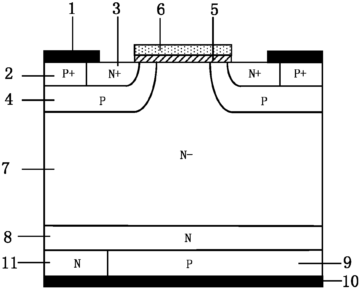
[0036] This embodiment provides a dual-channel RC-IGBT with a voltage level of 600V, and its cell structure is as follows figure 2 As shown, it includes emitter structure, gate structure, collector structure and drift region structure. The emitter structure includes metal emitter 1, P+ ohmic contact region 2, N+ emitter region 3 and P-type base region 4, where P+ The ohmic contact region 2 and the N+ emitter region 3 are independently arranged in the P-type base region 4, and the surfaces of the P+ ohmic contact region 2 and the N+ emitter region 3 are in contact with the metal emitter 1; the drift region structure includes N- The drift region 7 and the N-type electric field stop layer 8, the N-type electric field stop layer 8 is arranged on the back of the N-drift region 7; the gate structure includes a gate electrode 6 and a gate oxide layer 5, and the gate electrode 6 and N+ A gate oxide layer 5 is arranged between the emitter region 3, the P-type base region 4 and the N-d...

Embodiment 2

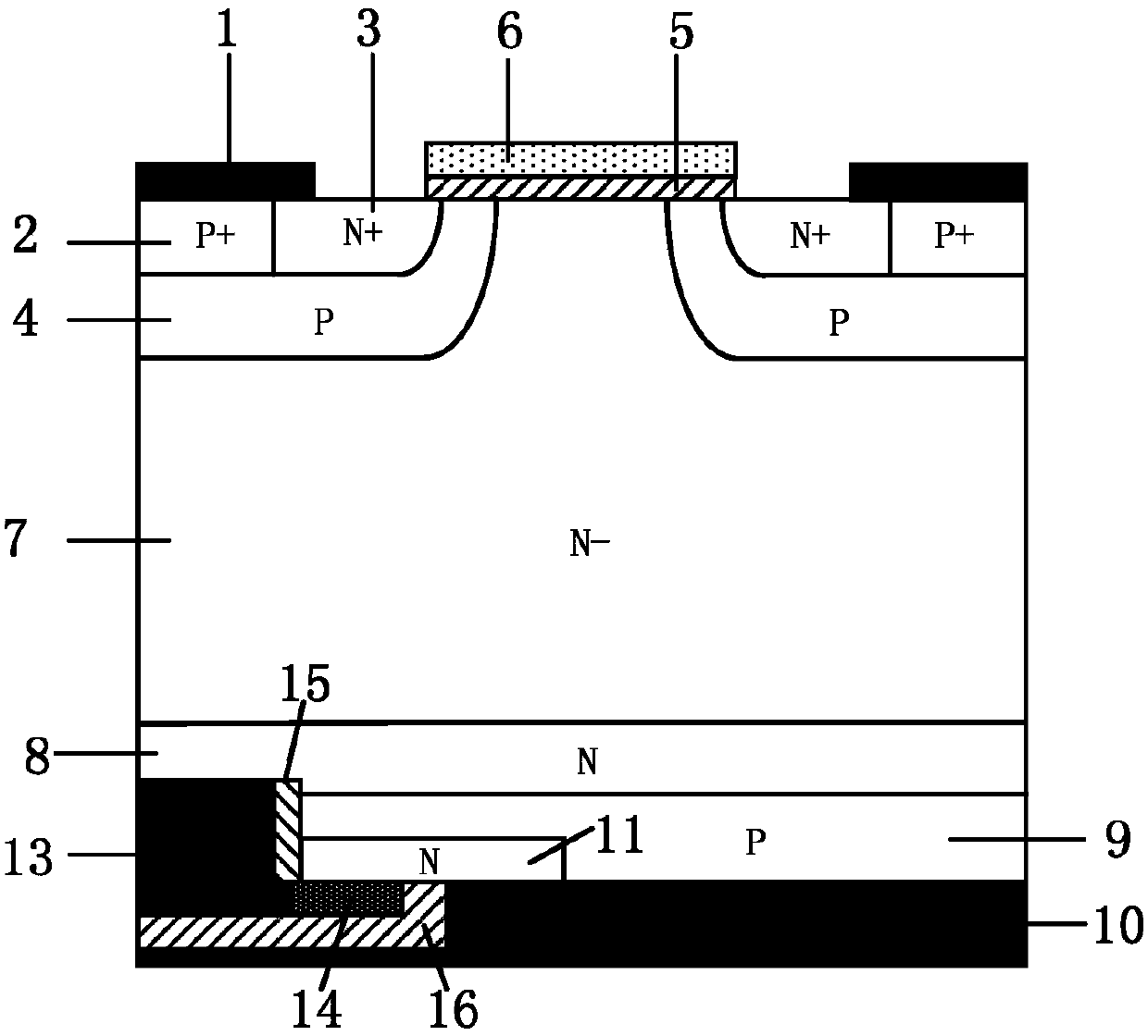
[0039] This embodiment provides a dual-channel RC-IGBT with a voltage level of 600V, and its cell structure is as follows image 3 As shown, this structure is based on Embodiment 1, and an N-type collector bypass region 12 is also provided between the N-type electric field stop layer 8 and the ohmic contact metal 13, and the N-type collector The front side of the bypass region 12 is in contact with the back side of the N-type electric field stop layer 8 , and the back side of the N-type collector bypass region 12 is connected to the ohmic contact metal 13 to form an ohmic contact. The thickness of the N-type collector bypass region 12 is also 0.1-0.3 microns smaller than the thickness of the P-type collector region 9, but compared with the N-type collector region 11, its thickness and doping concentration can be the same or different .

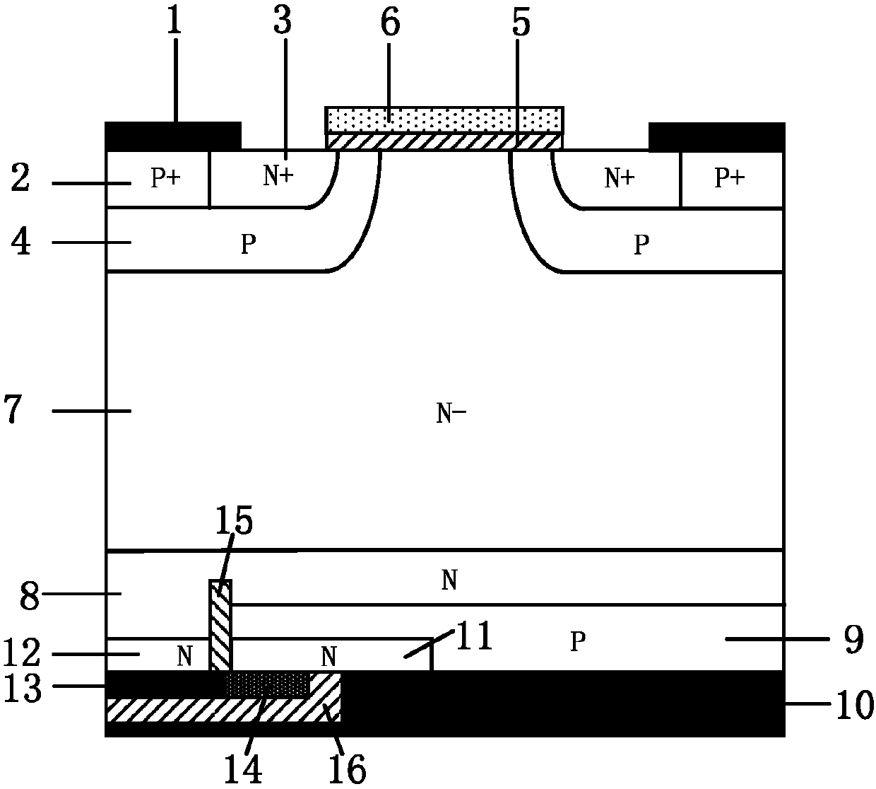
[0040] The preparation method of above-mentioned dual-channel RC-IGBT, such as Image 6 As shown, it specifically includes the following st...


PUM


Abstract

A dual-channel RC-IGBT device and a preparation method thereof. The invention belongs to the technical field of power semiconductor devices, and specifically provides a reverse conduction type insulated gate bipolar transistor (RC-IGBT) and a preparation method thereof, which are used to obtain better device characteristics and improve the reliability of the RC-IGBT; Based on the traditional RC‑IGBT device structure, through the introduction of structures such as dielectric trenches and Schottky contacts on the back of the device, the RC‑IGBT device completely eliminates the snapback phenomenon in the forward IGBT working mode, and has the same characteristics as the traditional IGBT It has a small conduction voltage drop in the reverse diode freewheeling mode; at the same time, since there is no need to increase the width of the back P+ collector area, a small rear cell width can be used, which solves the problem of traditional RC‑IGBT devices The problem of current and temperature uniformity greatly improves the reliability, and its preparation process is compatible with the traditional RC-IGBT device process.

Description

technical field [0001] The invention belongs to the technical field of power semiconductor devices, and relates to an insulated gate bipolar transistor (IGBT), in particular to a reverse conduction type insulated gate bipolar transistor (RC-IGBT) and a preparation method thereof. Background technique [0002] Insulated Gate Bipolar Transistor (IGBT) is a new type of power electronic device combining MOS field effect and bipolar transistor. It not only has the advantages of easy driving and simple control of MOSFET, but also has the advantages of low conduction voltage of power transistor, large on-state current and small loss. It has become one of the core electronic components in modern power electronic circuits and is widely used in Various fields of the national economy such as communications, energy, transportation, industry, medicine, household appliances and aerospace. The application of IGBT plays an extremely important role in improving the performance of power elec...

Claims


Application Information

Patent Timeline
Patent Type & Authority Patents(China)
IPC IPC(8): H01L29/739H01L21/331H01L29/08H01L29/06
CPCH01L29/06H01L29/0821H01L29/66325H01L29/7393
Inventor 张金平熊景枝郭绪阳廖航刘竞秀李泽宏任敏张波
Owner UNIV OF ELECTRONICS SCI & TECH OF CHINA
Why Eureka
Try Eureka