A superjunction igbt device with mixed conduction modes

A device and mode technology, applied in the field of insulated gate bipolar transistors, can solve the problems of IGBT not being fully turned on, reliability problems, etc.

Active Publication Date: 2020-11-13
UNIV OF ELECTRONICS SCI & TECH OF CHINA
View PDF6 Cites 0 Cited by
  • Summary
  • Abstract
  • Description
  • Claims
  • Application Information

AI Technical Summary

Problems solved by technology

SJ-RC-IGBT with RC structure such as image 3 As shown, but in the forward conduction, when its conduction mode is converted from unipolar to bipolar, there will be a negative resistance (Snapback) phenomenon, which will prevent the IGBT from being fully turned on when it is applied in parallel, so there is a problem in reliability. question

Method used


Image

  • A superjunction igbt device with mixed conduction modes
  • A superjunction igbt device with mixed conduction modes
  • A superjunction igbt device with mixed conduction modes

Examples


Embodiment 1

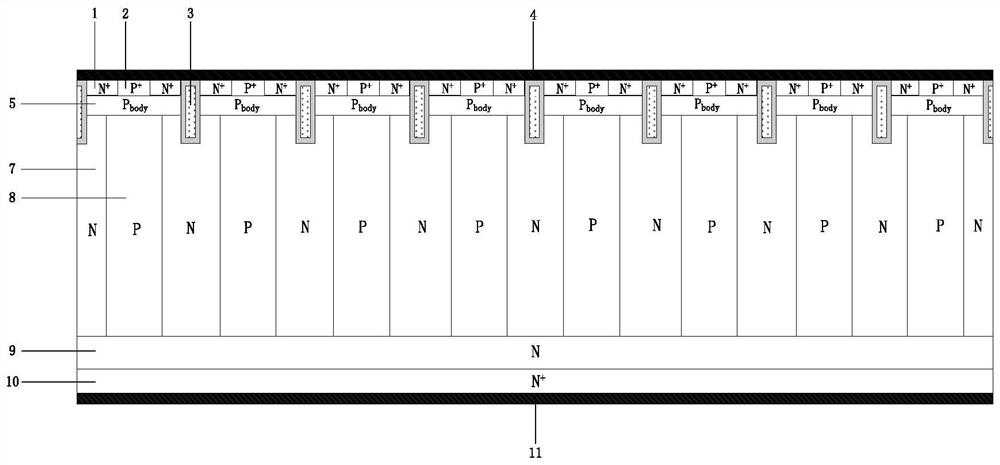
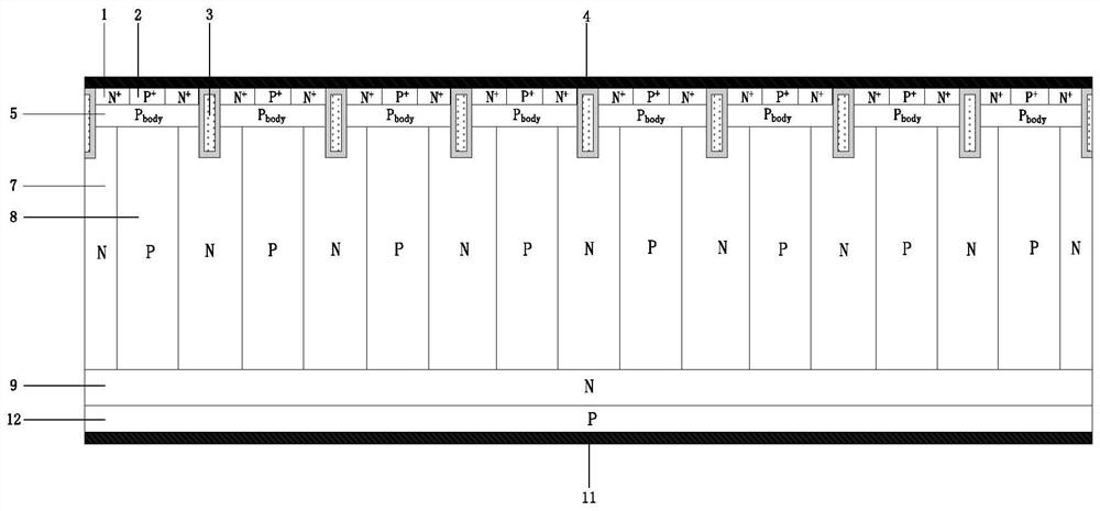
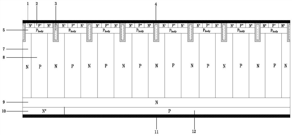
[0046] A superjunction IGBT device with a mixed conduction mode, comprising N+ collector regions 10 and P-type collector regions 12 arranged alternately, with N-type buffers on the upper surfaces of the N+ collector regions 10 and P-type collector regions 12 Layer 9, the upper surface of the N-type buffer layer 9 has a super junction drift region composed of a super junction N column region 7 and a super junction P column region 8, and the surface of the super junction drift region is composed of an N+ source region 1, a P+ A trench MOS structure consisting of a contact region 2, a polysilicon gate electrode 3, an emitter 4, and a Pbody base region 5 has a collector electrode 11 on the lower surface of the device, and between the N+ collector region 10 and the P-type collector region 12 There is a silicon dioxide layer 13 between them, the lower surface of the silicon dioxide layer 13 is in contact with the collector electrode 11, and the upper surface of the silicon dioxide la...

Embodiment 2

[0048] Such as Figure 5 As shown, the difference between this example and Example 1 is that the trench MOS structure is a planar gate structure.

Embodiment 3

[0050] Such as Figure 6 As shown, the difference between this example and Example 1 is that there is an N-type carrier storage layer 6 between the superjunction drift region and the surface MOS structure Pbody base region 5, and the N-type carrier storage layer The concentration of 6 is not less than that of the superjunction N-column region 7. Compared with Embodiment 1, this embodiment can further reduce the turn-on voltage drop and improve the turn-off performance of the device.


PUM


Abstract

The invention provides a superjunction IGBT device with a mixed conduction mode, comprising a superjunction composed of alternately arranged N+ collector regions and P-type collector regions, an N-type buffer layer, a superjunction N-column region and a super-junction P-column region Drift region, trench MOS structure, silicon dioxide layer, the upper surface of the silicon dioxide layer goes deep into the N-type buffer layer and the super junction drift region and is in contact with the super junction P column region, and the silicon dioxide layer connects the super junction P column region The N-type buffer layers on both sides are isolated; the super-junction drift region is not in contact with the surface MOS structure Pbody base region. A super-junction IGBT with a mixed conduction mode proposed by the present invention can completely eliminate the traditional SJ-RC through simulation verification. ‑IGBT Snapback phenomenon, and can be adjusted by N + collector area with P + The area ratio of the collector area changes the ratio of the two parts of SJ-VDMOS and SJ-IGBT, so that it has the advantages of both SJ-VDMOS and SJ-IGBT, and at the same time realizes the integration of anti-parallel diodes and improves the overall performance of the device.

Description

technical field [0001] The invention relates to an insulated gate bipolar transistor (IGBT) in the technical field of power semiconductor devices, in particular to a super junction IGBT device with a mixed conduction mode. Background technique [0002] VDMOS (Vertical Double-diffusion Metal-Oxide-Semiconductor) is a multi-subconductor device. Compared with bipolar transistors, it has fast switching speed, low switching loss, and good frequency characteristics; at the same time, it has the advantages of ordinary MOS devices: High input impedance and low driving power. In addition, due to the characteristics of its own structure, an anti-parallel diode is integrated inside, making its application easier. Due to the above advantages, VDMOS has been widely used in the fields of motor speed regulation, inverter, switching power supply, electronic switch, high-fidelity audio and so on. But its on-resistance and breakdown voltage meet: R ON ∝BV 2.5 , as the withstand voltage of...

Claims


Application Information

Patent Timeline
Patent Type & Authority Patents(China)
IPC IPC(8): H01L29/06H01L29/08H01L29/739
CPCH01L29/0634H01L29/0653H01L29/0843H01L29/7397H01L29/7398
Inventor 张金平赵倩刘竞秀李泽宏任敏张波
Owner UNIV OF ELECTRONICS SCI & TECH OF CHINA
Why Eureka
Try Eureka