A kind of rc-igbt device and preparation method thereof

A technology of device and collector area, which is applied in the field of power semiconductor devices, can solve problems affecting the reliability of RC-IGBT devices, current concentration and temperature unevenness, and increase the conduction voltage drop of diodes, so as to solve the problem of current and temperature uniformity The problem of good forward conduction voltage drop and short-circuit loss, the effect of low IGBT forward conduction voltage drop

Active Publication Date: 2019-05-14
UNIV OF ELECTRONICS SCI & TECH OF CHINA
View PDF4 Cites 0 Cited by
  • Summary
  • Abstract
  • Description
  • Claims
  • Application Information

AI Technical Summary

Problems solved by technology

However, this method has the following problems: 1) When the forward IGBT is turned on: it is difficult to completely eliminate the Snapback phenomenon due to the existence of the parasitic VDMOS, and the existence of the N-type collector region 11 makes the turn-on voltage drop of the traditional RC-IGBT larger than that of the traditional IGBT The conduction voltage drop, and the increased width of the P+ collector area will cause the current uniformity of the device when the forward IGBT is turned on, resulting in serious current concentration and uneven temperature, which seriously affects the reliability of the RC-IGBT device ; 2) When the reverse diode freewheeling conduction: the increased P+ collector area width increases the extraction of the P-type collector area 9 to the holes injected in the N-drift region 7, and increases the path of the current at the same time, increasing the diode The conduction voltage drop, and the increased width of the P+ collector region will cause the current uniformity problem of the device during the reverse diode freewheeling, resulting in serious current concentration and uneven temperature, which seriously affects the reliability of the RC-IGBT device

Method used


Image

  • A kind of rc-igbt device and preparation method thereof
  • A kind of rc-igbt device and preparation method thereof
  • A kind of rc-igbt device and preparation method thereof

Examples


Embodiment Construction

[0030] The principles and characteristics of the present invention will be further described below in conjunction with the accompanying drawings, and the examples given are only for explaining the present invention, and are not intended to limit the scope of the present invention.

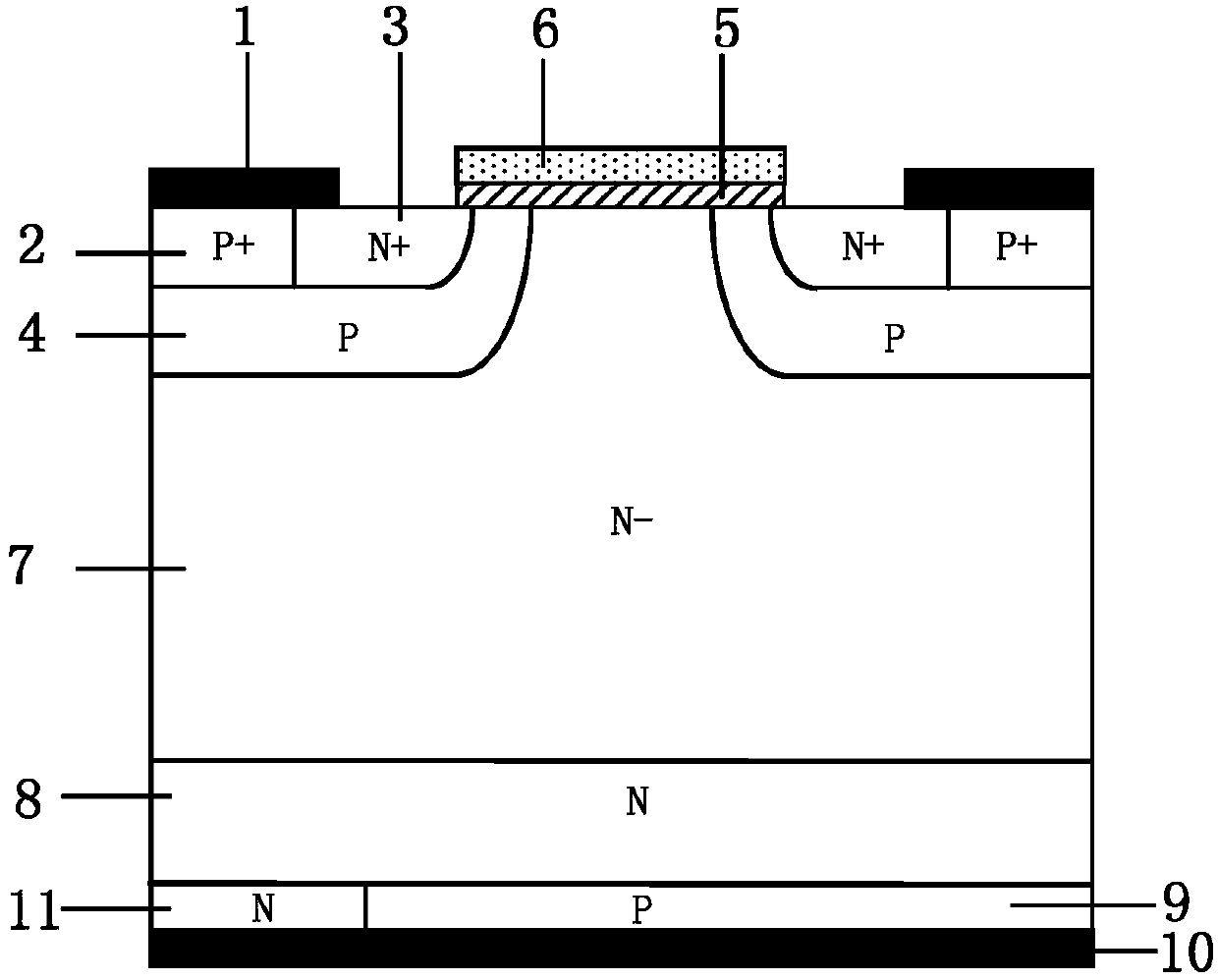
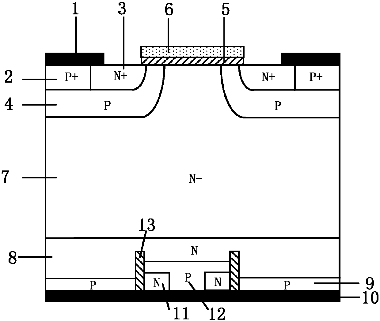
[0031] This embodiment provides an RC-IGBT device with a voltage level of 600V, and its cell structure is as follows figure 2 As shown, it includes emitter structure, gate structure, collector structure and drift region structure. The emitter structure includes metal emitter 1, P+ ohmic contact region 2, N+ emitter region 3 and P-type base region 4, where P+ The ohmic contact region 2 and the N+ emitter region 3 are independently arranged in the P-type base region 4, and the surfaces of the P+ ohmic contact region 2 and the N+ emitter region 3 are in contact with the metal emitter 1; the drift region structure includes N- The drift region 7 and the N-type electric field stop layer 8, the N-type el...


PUM


Abstract

The invention belongs to the technical field of power semiconductor devices, and specifically provides a reverse conduction insulated gate bipolar transistor (RC-IGBT) and a preparation method thereof, which are used to obtain better device characteristics and improve the reliability of the RC-IGBT; Invented RC-IGBT device completely eliminates the snapback phenomenon in the forward IGBT working mode, and because of the use of two P-type collector regions with different concentrations and thicknesses, lower IGBT forward conduction voltage drop and better A compromise between the forward conduction voltage drop and the short-circuit loss; in the reverse diode freewheeling mode, it has a small conduction voltage drop; at the same time, it is not necessary to increase the back P+ set in the case of parallel connection of multiple MOS cells on the front The width of the electrical area can be small, which solves the problem of current and temperature uniformity of traditional RC‑IGBT devices, greatly improves reliability, and its preparation process is compatible with traditional RC‑IGBT device processes.

Description

technical field [0001] The invention belongs to the technical field of power semiconductor devices, and relates to an insulated gate bipolar transistor (IGBT), in particular to a reverse conduction type insulated gate bipolar transistor (RC-IGBT) and a preparation method thereof. Background technique [0002] Insulated Gate Bipolar Transistor (IGBT) is a new type of power electronic device combining MOS field effect and bipolar transistor. It not only has the advantages of easy driving and simple control of MOSFET, but also has the advantages of low conduction voltage of power transistor, large on-state current and small loss. It has become one of the core electronic components in modern power electronic circuits and is widely used in Various fields of the national economy such as communications, energy, transportation, industry, medicine, household appliances and aerospace. The application of IGBT plays an extremely important role in improving the performance of power elec...

Claims


Application Information

Patent Timeline
Patent Type & Authority Patents(China)
IPC IPC(8): H01L29/739H01L29/417H01L21/331H01L21/28
CPCH01L29/401H01L29/41708H01L29/66333H01L29/7395
Inventor 张金平熊景枝廖航刘竞秀李泽宏任敏张波
Owner UNIV OF ELECTRONICS SCI & TECH OF CHINA
Why Eureka
Try Eureka