A method for manufacturing a multi-slot gate lateral high-voltage power device

A technology for power devices and manufacturing methods, which is applied in semiconductor/solid-state device manufacturing, semiconductor devices, electrical components, etc., can solve the problems of slow device turn-off speed, device latch-up effect, and reduction of forward conduction voltage drop, etc. Achieve low turn-off loss, fast turn-off speed, and high compatibility

Active Publication Date: 2020-08-28
UNIV OF ELECTRONICS SCI & TECH OF CHINA +1
View PDF5 Cites 0 Cited by
  • Summary
  • Abstract
  • Description
  • Claims
  • Application Information

AI Technical Summary

Problems solved by technology

[0003] As a bipolar device, the LIGBT device will have a conductance modulation effect when it is turned on, and a large number of carriers will be stored in the drift region. The problem of increased loss
In addition, the presence of parasitic thyristors in the body may cause latch-up of the device, thereby limiting the safe operating area

Method used


Image

  • A method for manufacturing a multi-slot gate lateral high-voltage power device
  • A method for manufacturing a multi-slot gate lateral high-voltage power device
  • A method for manufacturing a multi-slot gate lateral high-voltage power device

Examples


Embodiment 1

[0032] The manufacturing process of the multi-groove gate SOI LIGBT device in this example is as follows:

[0033] A method for manufacturing multi-groove gate SOI LIGBT, characterized in that it comprises the following steps:

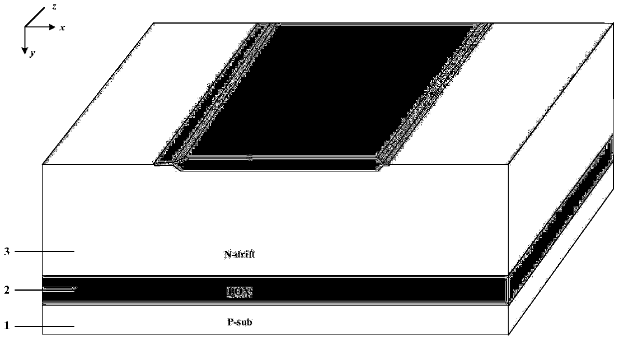
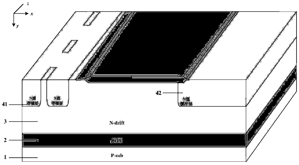
[0034] The first step: preparing SOI material, the SOI material includes bottom-up substrate layer 1, insulating dielectric layer 2 and N-type drift region 3, such as figure 1 shown;

[0035] Step 2: Implanting N-type impurities into one end of the surface of the N-type drift region 3 through ion implantation technology, and the impurity implantation windows are distributed in segmented patterns;

[0036] Step 3: Implanting N-type impurities into the other end of the surface of the N-type drift region 3 by ion implantation technology;

[0037] The fourth step: the second step and the third step of the ion-implanted N-type impurity are simultaneously subjected to high-temperature push-in junction, correspondingly forming the N-type storage layer 41 at...

Embodiment 2

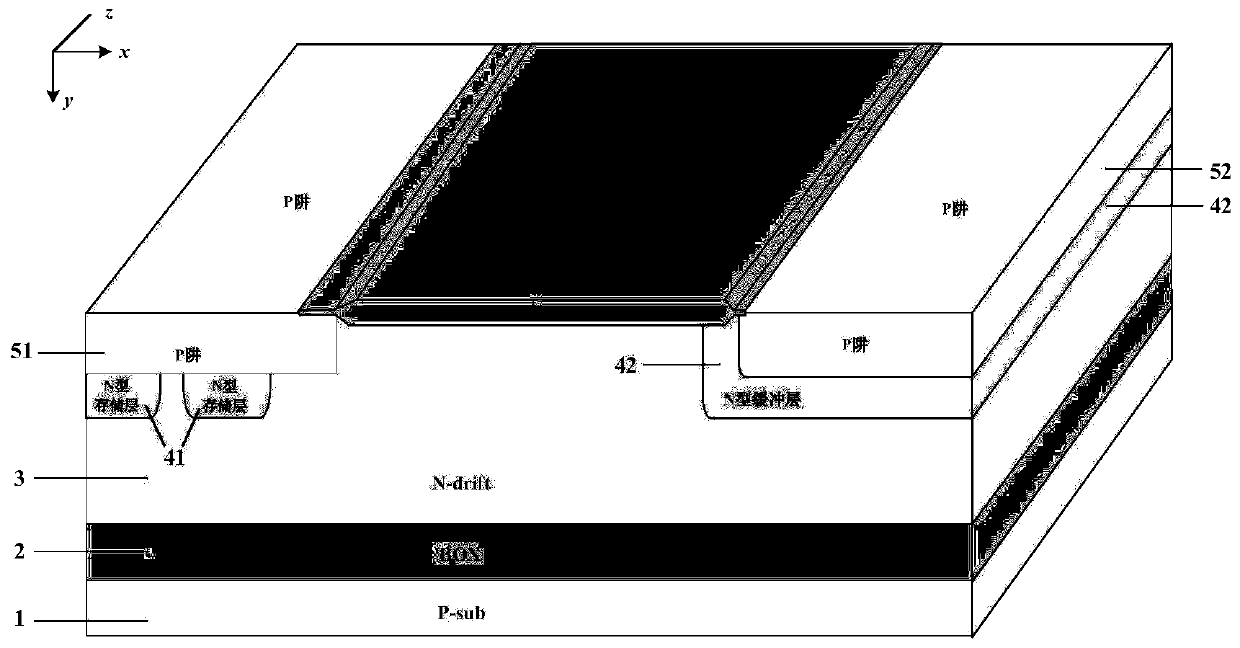
[0050] Such as Figure 8 Shown, in this example and embodiment 1 Figure 4 The difference is that in the eighth step of this example, the emitter end controls the bottom of the groove gate and the bottom of the blocking groove gate is implanted to form a P-type buried layer 53 . The working mechanism of device shutdown in this embodiment is consistent with that of Embodiment 1, the difference is that: when conducting forward conduction, the P-type buried layer 53 introduced in this example can assist in depleting the N-type storage layer 41, thereby improving the efficiency of the N-type storage layer. 41 Optimize the doping concentration and enhance the carrier storage effect, so in this example, the carrier concentration in the drift region of the device is higher, and the conduction voltage drop can be further reduced; at the same time, in the blocking state, the P-type buried layer 53 can also The electric field peak at the bottom of the emitter groove gate structure is r...

Embodiment 3

[0052] Such as Figure 9 and Figure 10 Shown, in this example and embodiment 1 Figure 7 The difference is that the layout of the emitter control grid and the collector grid can be intermittently distributed in rectangles or hexagons; Figure 11 It is shown that the emitter control slots and the collector slots are interconnected in a rectangular layout, of course, the emitter control slots and the collector slots may also be interconnected in a hexagonal layout. The device turn-off working mechanism in this embodiment is the same as that in Embodiment 1, the difference is that the shape of the groove gate can change the channel density of the device, which is beneficial to design the turn-on voltage drop and turn-off loss of the device.


PUM


Abstract

The invention belongs to the technical field of power semiconductors and particularly relates to a manufacturing method of a multi-trench gate lateral high-voltage power device. Compared with a traditional structure, a novel structure of the multi-trench gate lateral high-voltage power device has the advantages that an N-type storage layer at an emitter terminal, an N-type buffer layer at a collector terminal and P-type well regions at the emitter terminal and the collector terminal can be synchronously pushed via junctions separately to reduce the thermal budget cost of the device; and multi-trench gate structures at the emitter terminal and the collector terminal can also be synchronously manufactured and the multi-trench gate structures are formed at two ends of the device, thereby improving the conduction voltage drop and turn-off loss of the device. The manufacturing method has the beneficial effects that the process step is simplified, the process cost is reduced, and an easy-to-integrate and low-power SOI LIGBT is achieved.

Description

technical field [0001] The invention belongs to the technical field of power semiconductors, and relates to a method for manufacturing a multi-slot gate SOI LIGBT (Lateral Insulated Gate Bipolar Transistor, lateral insulated gate bipolar transistor). Background technique [0002] Insulated-gate bipolar transistor (IGBT) combines the advantages of high input impedance of MOS gate-controlled devices and low conduction voltage drop of bipolar devices to achieve high breakdown voltage and large conduction current, and has become a power electronic system Representative devices in the field, widely used in smart grid, high-speed rail drive, aerospace and household appliances and other fields. Due to the development of SOI technology, SOIL IGBT devices have smaller leakage currents and smaller parasitic effects, thus becoming the core components of monolithic power integrated chips. [0003] As a bipolar device, the LIGBT device will have a conductance modulation effect when it i...

Claims


Application Information

Patent Timeline
Patent Type & Authority Patents(China)
IPC IPC(8): H01L21/334H01L29/739
CPCH01L29/66348H01L29/7394H01L29/7397
Inventor 魏杰马臻黄俊岳王晨霞鲁娟郗路凡宋旭罗小蓉杨永辉朱坤峰
Owner UNIV OF ELECTRONICS SCI & TECH OF CHINA
Why Eureka
Try Eureka