Supercharge Your Innovation With Domain-Expert AI Agents!

PCB assembly and mobile terminal

A PCB board and component technology, which is applied in the field of PCB board components and mobile terminals, can solve the problems of antenna signal interference, occupying the space of the antenna clearance area, and reducing the space for arranging components, so as to improve the layout space and avoid interference.

Inactive Publication Date: 2016-11-09
GUANGDONG OPPO MOBILE TELECOMM CORP LTD
View PDF3 Cites 1 Cited by
  • Summary
  • Abstract
  • Description
  • Claims
  • Application Information

AI Technical Summary

Problems solved by technology

However, the setting of the antenna clearance area results in a smaller space for arranging components on the PCB, which is not conducive to the setting of more components on the PCB
In addition, due to the large size of some components, when the components are placed on the PCB, the components will be closer to the antenna clearance area or occupy a part of the antenna clearance area, which interferes with the antenna signal

Method used


Image

  • PCB assembly and mobile terminal
  • PCB assembly and mobile terminal

Examples


Embodiment Construction

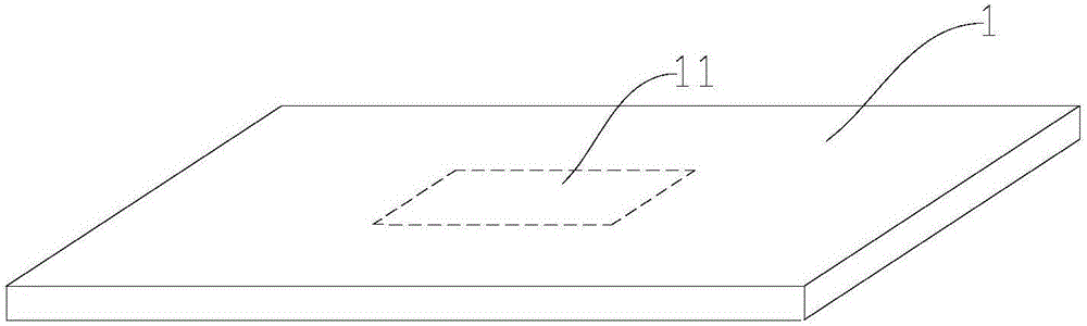
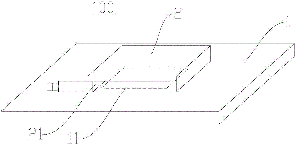
[0023] Embodiments of the invention are described in detail below, examples of which are illustrated in the accompanying drawings. The embodiments described below by referring to the figures are exemplary and are intended to explain the present invention and should not be construed as limiting the present invention.

[0024] In describing the present invention, it should be understood that the terms "length", "width", "thickness", "upper", "lower", "front", "rear", "left", "right", " The orientation or positional relationship indicated by "vertical", "horizontal", "top", "bottom", "inner", "outer", etc. is based on the orientation or positional relationship shown in the drawings, and is only for the convenience of describing the present invention and Simplified descriptions, rather than indicating or implying that the device or element referred to must have a particular orientation, be constructed and operate in a particular orientation, and thus should not be construed as lim...


PUM


Abstract

The invention discloses a PCB board assembly and a mobile terminal. The PCB board assembly includes an antenna; a first board body, the first board body is provided with an antenna clearance area, and the antenna is located in the antenna clearance area; a second board body, the second board is arranged on the first board, at least a part of the second board corresponds to the antenna clearance area, and the second board corresponds to the antenna clearance area There is a gap between the bottom wall and the antenna clearance area. According to the PCB board assembly of the present invention, the wiring can be routed on the side of the second board body away from the antenna clearance area so as to facilitate the arrangement of components on the second board body, thereby facilitating the improvement of the layout space of the components to be arranged on the PCB board assembly More components, while avoiding setting the components closer to the antenna clearance area or occupying a part of the antenna clearance area.

Description

technical field [0001] The invention relates to the technical field of mobile terminals, in particular to a PCB board assembly and a mobile terminal. Background technique [0002] In the related art, an antenna clearance area is usually provided on the PCB board. However, the arrangement of the antenna clearance area results in a smaller space for arranging components on the PCB, which is not conducive to the arrangement of more components on the PCB. In addition, due to the large size of some components, when the components are placed on the PCB, the components will be closer to the antenna clearance area or occupy a part of the antenna clearance area, which interferes with the antenna signal. Contents of the invention [0003] The present invention aims to solve one of the technical problems in the related art at least to a certain extent. For this reason, the present invention proposes a PCB board assembly, which is conducive to improving the layout space of component...

Claims


Application Information

Patent Timeline
IPC IPC(8): H01Q1/12H05K7/06
CPCH01Q1/12H05K7/06
Inventor 范艳辉
Owner GUANGDONG OPPO MOBILE TELECOMM CORP LTD
Features
  • R&D
  • Intellectual Property
  • Life Sciences
  • Materials
  • Tech Scout
  • Unparalleled Data Quality
  • Higher Quality Content
  • 60% Fewer Hallucinations
Learn More