Detection method of contact type ltps and pad structure used for the method

A detection method, contact technology, applied in the field of contact LTPS detection and pad structure, can solve the problems of wasting time, circuit failure, and the inability to judge product quality immediately, so as to control the measurement time and avoid heavy work Effect

Active Publication Date: 2020-01-17
EVERDISPLAY OPTRONICS (SHANGHAI) CO LTD
View PDF8 Cites 0 Cited by
  • Summary
  • Abstract
  • Description
  • Claims
  • Application Information

AI Technical Summary

Problems solved by technology

However, the probe contact measurement often has the problem of contact shift (contact displacement) because the design of the test pad 80 is not too large, and the positions of the probe 70 and the pad 80 cannot be accurately aligned.
like figure 2 and image 3 Shown are examples of two kinds of Contact shift, in figure 2 In the middle, because the angle of the probe 70 is tilted, it cannot be accurately aligned with the pad 80
exist image 3 In the middle, it is because the deviation of the probe 70 up, down, left, and right leads to the inability to accurately align with the pad 80
[0004] Therefore, in the current LTPS electrical testing, when contact shift occurs, if there is no loop 90 formed between the pads 80, it is impossible to test whether there is a problem with the probe lap; even if there is a loop formed between the pads 80 90, but if there is a problem in the product process that causes the loop to fail, and it is impossible to immediately determine whether it is a problem with the probe lap or a product quality problem, it is necessary to waste time and manually judge and analyze whether the contact shift is caused by the probe lap problem. It is caused by the quality problem of the product itself

Method used


Image

  • Detection method of contact type ltps and pad structure used for the method
  • Detection method of contact type ltps and pad structure used for the method
  • Detection method of contact type ltps and pad structure used for the method

Examples


Embodiment Construction

[0036] In order to make the object, technical solution and advantages of the present invention clearer, the present invention will be further described in detail below in conjunction with the accompanying drawings and embodiments. It should be understood that the specific embodiments described here are only used to explain the present invention, not to limit the present invention.

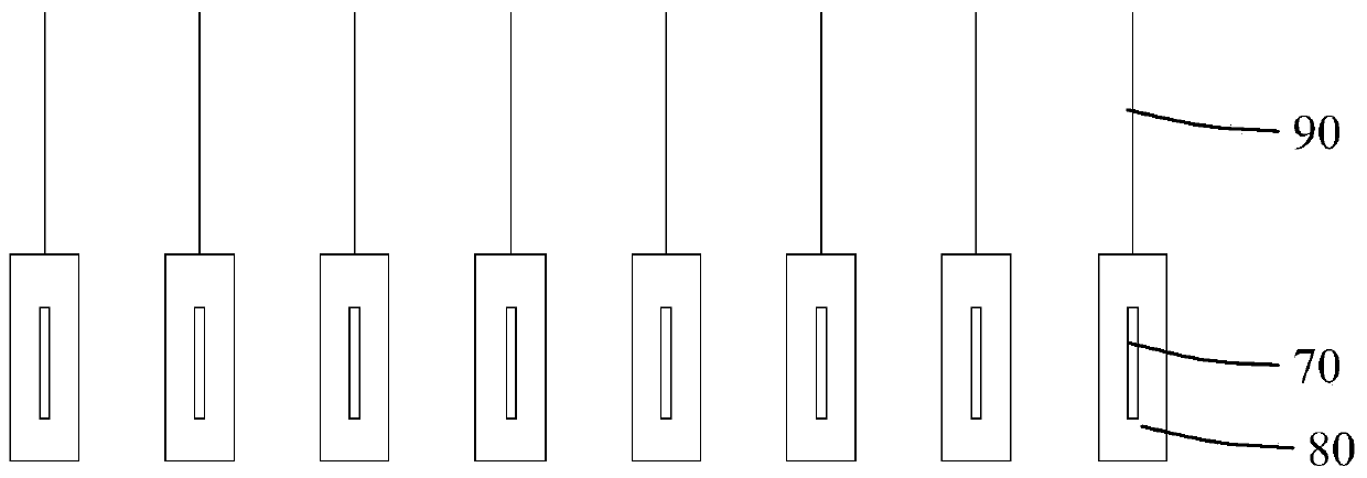
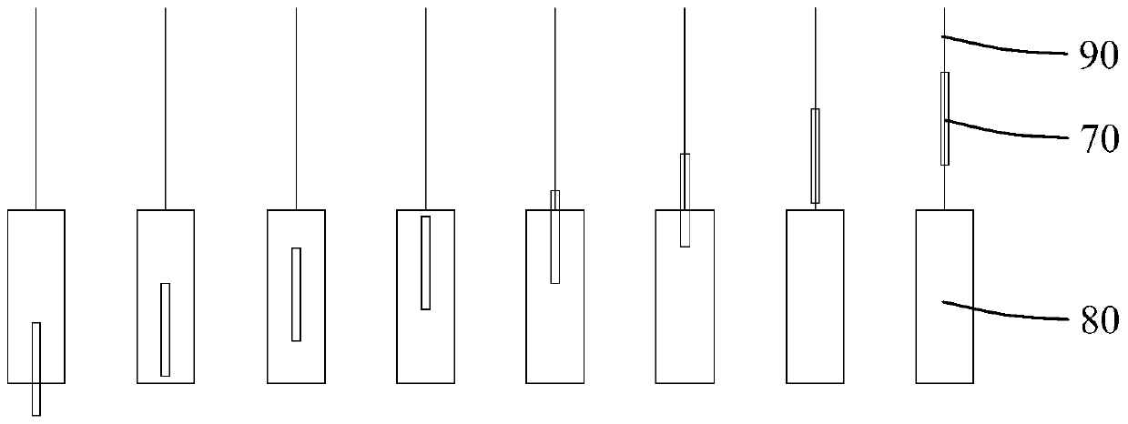
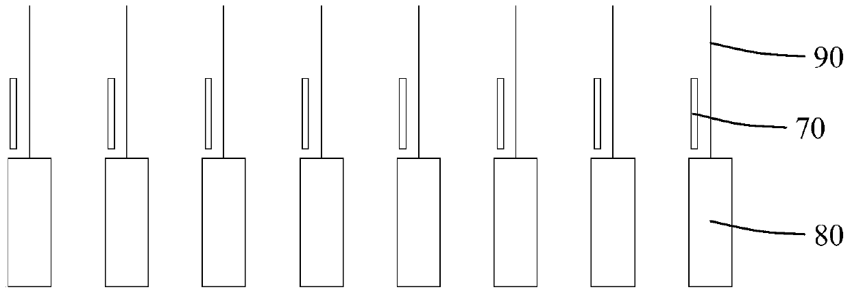
[0037] Cooperate with reference Figure 5 and Figure 6 As shown, the pad structure used for contact LTPS detection in the present invention includes a plurality of pads 20 to be tested, and a first test pad 110 and a second test pad 110 are arranged in the multiple pads 20 to be tested. The bonding pad 120 , the first testing bonding pad 110 and the second testing bonding pad 120 can be arranged at any position, and the first testing bonding pad 110 is electrically connected to the second testing bonding pad 120 . A loop 40 may be formed between each of the plurality of pads 20 to be tested, the...


PUM


Abstract

The invention provides a contact LTPS (Low Temperature Poly-silicon) detection method and a pad structure applied to contact LTPS detection. The detection method comprises the steps of providing an LTPS device, wherein the LTPS device comprises a plurality of pads to be detected; arranging a first test pad and a second test pad in the plurality of pads to be detected, and enabling the first test pad and the second test pad to be electrically connected; providing a probes, and enabling the probes to be lapped with the pads to be detected, the first test pad and the second test pad; applying voltage to the first test pad, measuring voltage of the second test pad, and thus determining a contact state of the probe and the corresponding pad to be detected. According to the invention, the first test pad and the second test pad are arranged in the plurality of pads to be detected of the LTPS device, if the voltage of the second test pad is measured in detection, it is proved that the probe and the corresponding pad are contacted normally; and if the voltage of the second test pad cannot be measured, it is proved that contact shift occurs between the probe and the corresponding pad.

Description

technical field [0001] The invention relates to the technical field of low-temperature polysilicon LTPS, in particular to a detection method of contact LTPS and a pad structure used in the method. Background technique [0002] Low temperature polysilicon technology LTPS (Low Temperature Poly-silicon) was originally developed to reduce the energy consumption of the Note-PC display and make the Note-PC appear thinner and lighter. This technology began to be tested in the mid-1990s stage. OLED, a new generation of organic light-emitting diode display panels derived from LTPS, also officially entered the practical stage in 1998. Its biggest advantages are ultra-thin, light weight, low power consumption, and can provide more vivid colors and clearer images. [0003] In the current LTPS electrical testing, there are contact measurement and non-contact measurement, such as figure 1 As shown, the contact measurement mostly uses the probe 70 to contact the pad (Pad) 80 of the LTPS ...

Claims


Application Information

Patent Timeline
Patent Type & Authority Patents(China)
IPC IPC(8): G01R31/50
Inventor 李原欣
Owner EVERDISPLAY OPTRONICS (SHANGHAI) CO LTD
Why Eureka
Try Eureka