Display base plate, display panel, manufacturing method of display base plate, manufacturing method of display panel, and display device
A display substrate, display panel technology, applied in the direction of instruments, semiconductor devices, optics, etc.
- Summary
- Abstract
- Description
- Claims
- Application Information
AI Technical Summary
Problems solved by technology
Method used
Image

Examples
Embodiment Construction
[0053] In order to make the purpose, technical solutions and advantages of the embodiments of the present invention more clear, the technical solutions of the embodiments of the present invention will be further described in detail below in conjunction with the accompanying drawings.
[0054] The components or elements shown in the accompanying drawings are marked as follows:
[0055] 1, 2, 3 display panels;
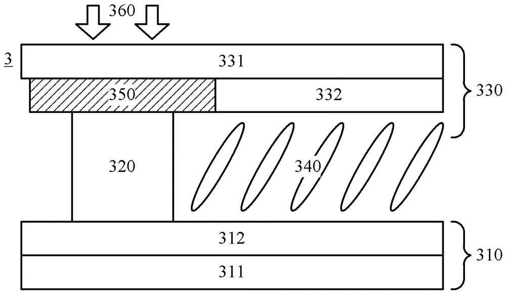
[0056] 110, 210, 310 opposing substrates;
[0057] 111, 211, 311 a first substrate substrate;
[0058] 112, 212, 312 thin film transistor layers;
[0059] 120, 220, 320 frame sealant;
[0060] 130, 230, 330 display substrate;
[0061] 131, 231, 331 a second substrate substrate;
[0062] 132, 232, 313, 332 color filter layers;
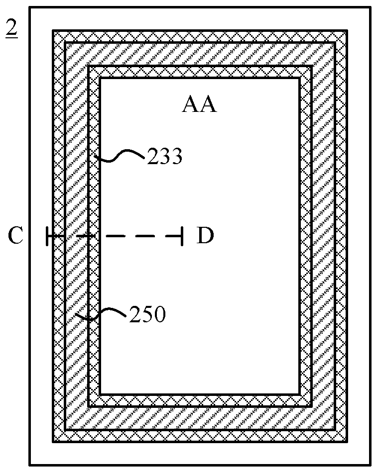
[0063] 133, 233, 314 black matrix;
[0064] 140, 240, 340 liquid crystal layer;
[0065] 250, 350 curing energy transmission layer;
[0066] 160, 260, 360, 360' solidifying energy beams; and
[0067] AA display area.
[0068] Figure 1A...
PUM
| Property | Measurement | Unit |
|---|---|---|
| transmittivity | aaaaa | aaaaa |
Abstract
Description
Claims
Application Information
 - R&D Engineer
- R&D Manager
- IP Professional
- Industry Leading Data Capabilities
- Powerful AI technology
- Patent DNA Extraction
Browse by: Latest US Patents, China's latest patents, Technical Efficacy Thesaurus, Application Domain, Technology Topic.
© 2024 PatSnap. All rights reserved.Legal|Privacy policy|Modern Slavery Act Transparency Statement|Sitemap