Supercharge Your Innovation With Domain-Expert AI Agents!

Programmable Non-Volatile Memory and Its Application in Semiconductor Storage Devices

A non-volatile, memory technology, applied in the direction of semiconductor devices, electric solid state devices, electrical components, etc., to achieve the effect of high write life and high data retention life

Inactive Publication Date: 2019-02-15
SICHUAN HONGXINWEI TECH
View PDF10 Cites 0 Cited by
  • Summary
  • Abstract
  • Description
  • Claims
  • Application Information

AI Technical Summary

Problems solved by technology

They also point out that the local power consumption during write and erase operations is so important that they will eventually be the limit of the write endurance parameter

Method used


Image

  • Programmable Non-Volatile Memory and Its Application in Semiconductor Storage Devices
  • Programmable Non-Volatile Memory and Its Application in Semiconductor Storage Devices
  • Programmable Non-Volatile Memory and Its Application in Semiconductor Storage Devices

Examples


Embodiment 1

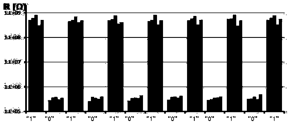
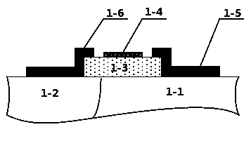
[0028] figure 1 In the most basic embodiment of the memory cell of the present invention, a diode comprising a substrate having a resistivity of about 1 Ω·cm and a thickness of about 1 μm. An anode region 1-1 of the p-type silicon layer and a cathode region 1-2 of the n-type silicon layer are respectively formed on the substrate. The aluminosilicate glass layer 1-3 is formed on the termination surface of the pn junction between the p-type anode region 1-1 and the n-type cathode region 1-2, and the doping concentration is 8*10 16 -2*10 17 cm -3 Na. It is covered with a 0.5um thick Ti-N-Si resistance heater 1-4, and the metal contacts 1-5, 1-6 are respectively connected to the anode area 1-1 and the cathode area 1-2. Standard mesa fabrication methods and techniques are used to form the described structures.

[0029] In the specific operation, the aluminosilicate glass layer 1-3 is heated by the resistance heater 1-4 covered above to increase the mobility of Na ions in it, a...

Embodiment 2

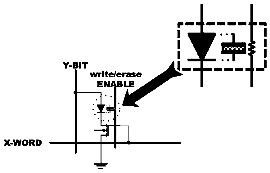
[0032] figure 2 As another basic embodiment of the memory cell of the present invention, a MOS transistor includes a p-type silicon substrate 2-1 with a resistivity of about 1Ω·cm and a thickness of about 1 μm, and an n-type silicon substrate formed on the substrate 2-1. type of source region 2-2 and drain region 2-3. The aluminosilicate layer 2-4 (gate insulating layer) is about 0.5 μm thick, and the doping concentration is 8*10 16 -2*10 17 cm -3 Na, and covers part of the regions 2-1, 2-2, 2-3. The metal pole 2-5 and the resistance heater 2-6 made of Ti-N-Si are located on the aluminosilicate layer 2-4, and the metal contacts 2-7 and 2-8 are respectively connected to the source region 2-2 and drain regions 2-3, 0.8 μm thick SiO 2 Layer 2-9, covering the remainder of the top surface of substrate 2-1. The structures can be formed by mesa process methods and techniques.

[0033] In the specific operation, the aluminosilicate layer 2-4 is heated by the resistance heater ...


PUM


Abstract

A reprogrammable non-volatile memory, in order to improve data write life and maintain life, using ionic conductors as ionic memory storage. The ionic conductor is doped with alkaline ions and has a resistive heater adjacent thereto. It can be applied to reprogrammable non-volatile semiconductor devices. When it is applied to a semiconductor memory, at least a portion of the P-type conductive side of the PN junction termination surface of the semiconductor memory is covered with an ion conductor film doped with alkaline ions as an ion memory, and has a resistance heating layer adjacent thereto .

Description

technical field [0001] The present invention generally relates to a reprogrammable nonvolatile memory with ion storage, in particular to a reprogrammable nonvolatile semiconductor memory utilizing ion storage, suitable for reprogrammable high-density and capacity storage applications . More specifically, it relates to memory devices with flash memory architecture, unlimited write endurance (such as reprogramming cycle count), and extended data retention lifetime, especially at high temperatures. Background technique [0002] The currently known development of reprogrammable non-volatile semiconductor memory, whether it is phase change type, conductive bridge type, ferroelectric type, floating gate type or resistive type. Compared with storage density, retentivity, remanence, write-read-erase speed, and operating temperature range, write-erase cycle count or write life is an important indicator of reliability and requires special attention. [0003] In floating gate memory,...

Claims


Application Information

Patent Timeline
Patent Type & Authority Patents(China)
IPC IPC(8): H01L27/11521H01L27/11568
CPCH10B69/00
Inventor 李学良西里奥·艾·珀里亚科夫
Owner SICHUAN HONGXINWEI TECH
Features
  • R&D
  • Intellectual Property
  • Life Sciences
  • Materials
  • Tech Scout
  • Unparalleled Data Quality
  • Higher Quality Content
  • 60% Fewer Hallucinations
Learn More