Method for manufacturing printed circuit board through enhancing semi-additive process

A technology of semi-additive method and production method, applied in the directions of printed circuit, printed circuit manufacturing, conductive pattern formation, etc., can solve the problems of limiting circuit thickness and low dry film thickness, etc.

Active Publication Date: 2017-01-04
广东佛智芯微电子技术研究有限公司
View PDF4 Cites 17 Cited by
  • Summary
  • Abstract
  • Description
  • Claims
  • Application Information

AI Technical Summary

Problems solved by technology

The improvement of the number of turns density limits the line width and line spacing of the line, so the improvement of the cross section can only be realized by increasing the line height as much as possible
[0008] If the subtractive method is used, the undercut effect will become very obvious when manufacturing fine lines with high copper thickness; if the semi-additive method is used, a dry film with good resolution needs to be used, but the thickness of such dry film is often very low, which in turn limits the thickness of the line

Method used


Image

  • Method for manufacturing printed circuit board through enhancing semi-additive process
  • Method for manufacturing printed circuit board through enhancing semi-additive process
  • Method for manufacturing printed circuit board through enhancing semi-additive process

Examples


Embodiment 1

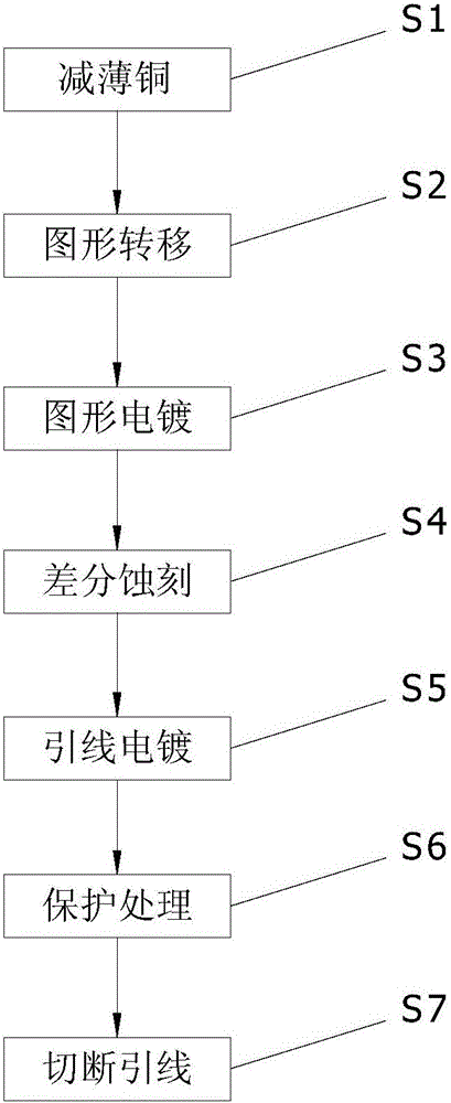
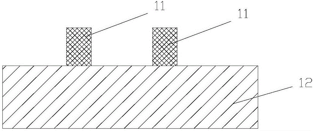
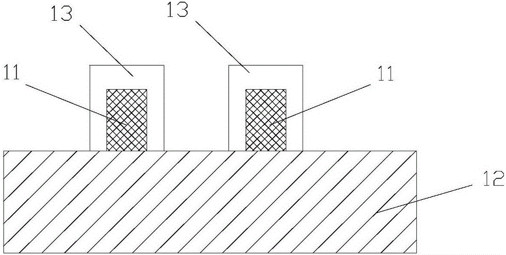
[0036] see Figure 1 to Figure 3 , a method of manufacturing a printed circuit board using an enhanced semi-additive method of the present embodiment, comprising the following steps:

[0037] Step S1: Copper Thinning

[0038] Prepare a double-sided copper-clad laminate, which has copper layers on both sides of the insulating substrate. The thickness of the insulating substrate is 50 μm, and the copper thickness is 12 μm. After cutting the double-sided copper-clad laminate, the size is 250×210mm 2 .

[0039] Copper thinning treatment is carried out on the copper clad laminate, and the copper thinning treatment is carried out with acidic copper reducing potion, so that the thickness of the copper layer is reduced to 5 μm.

[0040] Make through holes on the thinned copper clad laminate by mechanical drilling and laser drilling; the hole diameter is 100 μm, and then remove the residue and stains in the holes.

[0041] The copper-clad laminate is first processed through the blac...

Embodiment 2

[0056] The steps of this embodiment are basically the same as those of Embodiment 1, the difference is that this embodiment uses a single-sided copper clad laminate, the thickness of the insulating substrate is 50 μm, and the copper thickness is 12 μm; the copper thinning treatment is carried out by mechanical means, so that the thickness of the copper layer Thinning to 7 μm, the mechanical method is grinding or polishing; the blind hole is made by laser drilling on the thinned copper clad laminate, and the diameter of the blind hole is 150 μm; when making the electroplating seed layer, first use electroless copper, Make the copper thickness greater than 3μm, and then flash-plate until the copper thickness reaches 5~7μm; use a dry film with a thickness of 20 μm, and the line thickness in the pattern plating step is 20 μm, and after differential etching, the line width in the circuit pattern is 5 μm , the line spacing is 33 μm, and the line height is 20 μm; after lead plating, t...

Embodiment 3

[0058] The steps of this embodiment are basically the same as those of Embodiment 1, the difference is that this embodiment uses double-sided copper clad laminates, the thickness of the insulating substrate is 50 μm, and the copper thickness on both sides is 12 μm; the copper thinning treatment adopts acidic chemical copper reduction To reduce the thickness of the copper layer to 1 μm; make through holes on the thinned copper clad laminate by laser drilling; when making the electroplating seed layer, first use electroless copper to make the copper thickness greater than 3 μm, and then flash Plating until the copper thickness reaches 5~7μm; use a dry film with a thickness of 20 μm, and the thickness of the line in the pattern plating step is 25 μm. After differential etching, the line width in the line pattern is 20 μm, the line spacing is 112 μm, and the line height is 20 μm ; After lead plating, the line width is 32 μm, the line spacing is 100 μm (500% of the dry film resoluti...


PUM


Abstract

The invention discloses a method for manufacturing a printed circuit board through an enhancing semi-additive process. The method comprises the following steps: 1) thinning copper: performing thinning copper treatment on a copper-clad plate, forming a through hole or blind hole, and then manufacturing an electroplating seed layer; 2) transferring pattern: pasting a photosensitive film, forming an electroplating barrier layer on the surface of the copper-clad plate through a pattern transferring method and designing a lead connecting circuit copper layer and a non-circuit copper layer while transferring the pattern; 3) electroplating the pattern: fully plating the blind hole or the through hole while electroplating and forming the circuit pattern; 4) differentially etching: removing the bare bottom copper through a differential etching method and remaining the circuit pattern; 5) electroplating wire: electroplating the circuit pattern through the wire, widening and heightening the circuit; 6) protecting treatment: forming a metal protection layer on the surface of the conductive circuit; 7) cutting off the wire. According to the method provided by the invention, the limitation of the resolution and thickness of the photosensitive film to the cross section of the circuit is broken through and the method is especially fit for manufacturing the fine circuit with high copper thickness.

Description

technical field [0001] The invention relates to the technical field of printed circuits, in particular to a method for manufacturing printed circuit boards using an enhanced semi-additive method. Background technique [0002] There are many manufacturing methods for manufacturing printed circuit boards, which can be classified into subtractive method, additive method and semi-additive method according to the process principle. [0003] Among them, the subtractive method is to selectively etch away the non-circuit area on the copper-clad substrate through the protection of the patterned dry film to form a conductive pattern, which is currently the most widely used and mature method; The method of forming a conductive pattern circuit on an insulating substrate, this method currently has a narrow application range, and most of them are in the research and development stage; the semi-additive method combines the advantages of the subtractive method and the additive method, that ...

Claims


Application Information

Patent Timeline
Patent Type & Authority Applications(China)
IPC IPC(8): H05K3/10
CPCH05K3/108H05K2203/072
Inventor 张仕通朱府杰李大树潘丽
Owner 广东佛智芯微电子技术研究有限公司
Why Eureka
Try Eureka