Wafer scanning detection location method

A scanning detection and positioning method technology, applied in the optical field, can solve the problems of positioning error, built-in time difference, etc., and achieve the effect of avoiding data stream storage, ensuring the realization of online detection, and preventing positioning errors

Inactive Publication Date: 2017-01-11
中国科学院嘉兴微电子仪器与设备工程中心
View PDF6 Cites 0 Cited by
  • Summary
  • Abstract
  • Description
  • Claims
  • Application Information

AI Technical Summary

Problems solved by technology

[0004] The embodiment of the present application solves the problem of positioning error caused by the built-in time difference between the sampling component and the positioning component in the prior art by providing a wafer scanning detection positioning method

Method used


Image

  • Wafer scanning detection location method

Examples


Embodiment 1

[0030] An embodiment of the present application provides a wafer scanning detection and positioning method, wherein the wafer is fixed on a mobile platform, and the mobile platform drives the wafer to move.

[0031] When the mobile platform starts to move, the positioning component is in working state.

[0032] After the mobile platform moves to a stable state, the sampling component starts to collect scattered light signals.

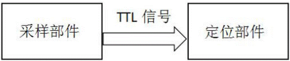
[0033] When the scattered light signal starts to be collected, the sampling component sends a TTL signal to the signal collection port connected to the positioning component.

[0034] After the signal collection port receives the TTL signal, the positioning component collects positioning information according to a predetermined frequency.

[0035] Wherein, the positioning component is a grating ruler built in the mobile platform.

[0036] The sampling component includes a photodetector, an analog-to-digital conversion card, and a data acquisition card...

Embodiment 2

[0043] An embodiment of the present application provides a wafer scanning detection positioning method, including the synchronization of the acquisition start time of the positioning component and the sampling component, and the synchronization of the sampling interval of the positioning component and the sampling component.

[0044] Synchronization of the acquisition start time of the positioning component and the sampling component: the wafer is fixed on the mobile platform, and the mobile platform drives the wafer to move; when the mobile platform starts to move, the positioning component is in a working state; the After the mobile platform moves to a stable state, the sampling part starts to collect scattered light signals; when the scattered light signals start to collect, the sampling part sends a TTL signal to the signal collection port connected to the positioning part; the signal collection After the port receives the TTL signal, the positioning component collects posi...

Embodiment 3

[0056] An embodiment of the present application provides a wafer scanning detection and positioning method, which can be divided into three aspects: synchronous sampling, trajectory positioning, and classification and storage of positioning information based on scattered light signals.

[0057] 1. Synchronous sampling:

[0058] Synchronous sampling includes the synchronization of the acquisition start time of the positioning component and the sampling component, and the synchronization of the sampling interval of the positioning component and the sampling component.

[0059] Synchronization of the acquisition start time of the positioning component and the sampling component: the wafer is fixed on the mobile platform, and the mobile platform drives the wafer to move; when the mobile platform starts to move, the positioning component is in working condition; the After the mobile platform moves to a stable state, the sampling part starts to collect scattered light signals; while...


PUM


Abstract

The invention belongs to the field of optical technology and discloses a wafer scanning detection location method, wherein a wafer is fixed on a moving platform, and the moving platform drives the wafer to move, a location part is at a working state while the moving platform starts to move, a sampling part starts to acquire a scattered light signal after the moving platform moves to a stable state, the sampling part transmits a TTL signal to a signal acquisition port connected with the location part while the scattered light signal starts to be acquired, and the location part locates information according to preset frequency after the signal acquisition port receives the TTL signal. The wafer scanning detection location method solves the problem in the prior art that the sampling part and the location part cause a location error because of built-in time difference. The synchronicity of the sampling part and the location part is implemented so as to guarantee the accurate location for scanning detection of a wafer.

Description

technical field [0001] The invention relates to the field of optical technology, in particular to a wafer scanning detection positioning method. Background technique [0002] Scanning inspection is realized based on the scattering behavior of wafer defects: a small beam of light spot is incident on a certain area of ​​the wafer. When there is no defect on the wafer surface, all the incident light will be reflected from the opposite direction at the same angle; when the irradiation area When there is a defect, part of the incident light will be converted into scattered light and emitted from all directions above the wafer, and the size of the defect affects the intensity of the scattered light, so as to judge the size of the defect. [0003] In the prior art, the sampling start time of the sampling part and the positioning part is aligned through the internal time, and there are inevitable errors in the internal time of these two parts. For high-throughput testing instruments...

Claims


Application Information

Patent Timeline
Patent Type & Authority Applications(China)
IPC IPC(8): G01N21/49G01B11/00
CPCG01N21/49G01B11/002
Inventor 陈鲁刘虹遥张朝前杨乐马砚忠路鑫超
Owner 中国科学院嘉兴微电子仪器与设备工程中心
Why Eureka
Try Eureka