
PCB structure

A technology for PCB boards and soldering pads, applied in the direction of electrical connection of printed components, printed circuit components, electrical components, etc., can solve problems such as low production efficiency, waste of labor costs, and tinning, so as to reduce and improve the soldering phenomenon. The effect of production efficiency and labor cost saving

Inactive Publication Date: 2017-02-08
PHICOMM (SHANGHAI) CO LTD
View PDF3 Cites 2 Cited by
  • Summary
  • Abstract
  • Description
  • Claims
  • Application Information

AI Technical Summary

Problems solved by technology

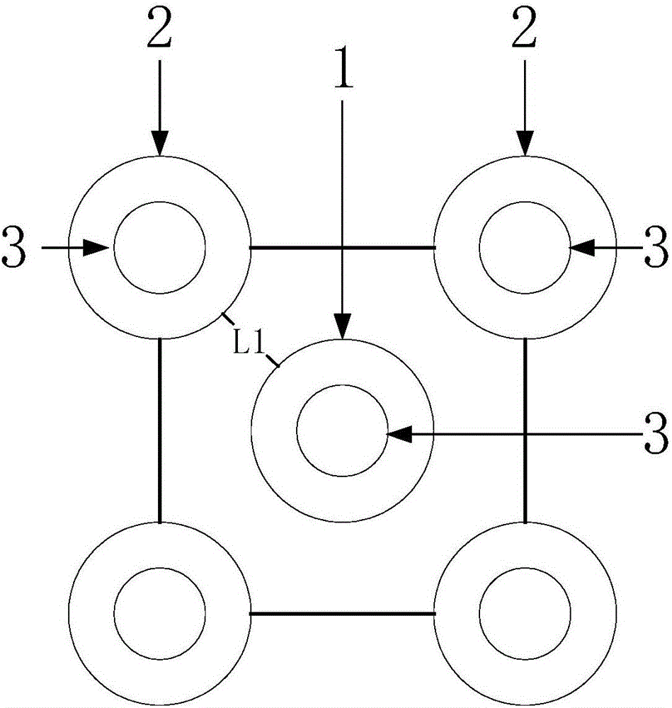
[0006] Wherein, the distance L1 between the existing center pad and the existing outer ring pad is 0.3mm or 0.35mm, however, in the actual production process, the distance between the existing center pad and the existing outer ring pad The distance between the two pads is set to 0.3 or 0.35 mm, so that the distance between the existing central pad and the existing outer ring pad is relatively close, and it is easy to cause a short circuit between the two pads, which will cause the existing central pad Soldering phenomenon occurs between the existing outer ring pads during wave soldering, which requires staff to manually remove tin, the production efficiency is still not high, and labor costs are also wasted

Method used


Image

  • PCB structure
  • PCB structure

Examples


Embodiment Construction

[0027] In the following description, numerous specific details are set forth in order to provide a thorough understanding of the present invention. However, the present invention can be implemented in many other ways different from those described here, and those skilled in the art can make similar extensions without violating the connotation of the present invention, so the present invention is not limited by the specific implementations disclosed below.

[0028] Secondly, the present invention is described in detail by means of schematic diagrams. When describing the embodiments of the present invention in detail, for convenience of explanation, the schematic diagrams are only examples, which should not limit the protection scope of the present invention.

[0029] In the drawings, the shapes of elements are exaggerated for clarity, and corresponding numerals refer to corresponding elements throughout. It will also be understood that when a layer is referred to as being on an...


PUM


Abstract

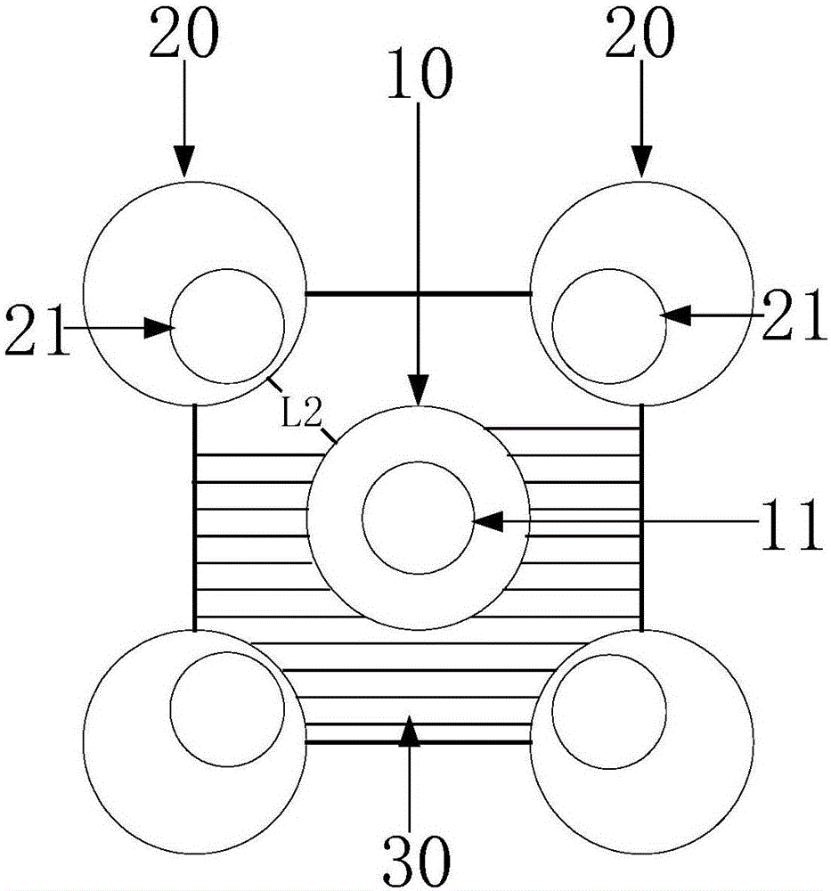
The present invention discloses a PCB structure. The structure comprises a main body and a bonding pad arranged on the main body; the bonding pad includes a group of bonding pads arranged at the fixed region of the main body, and the group of bonding pads include the centre bonding pads arranged on the fixed region of the main body and outer ring bonding pads arranged around the centre boding pads, wherein the distance between the outer ring bonding pads and the centre bonding pads is larger than or equal to 0.4mm. The distance between the outer ring bonding pads and the centre bonding pads is larger than or equal to 0.4mm to allow the tin connection phenomenon between the outer ring bonding pads arranged around the centre boding pads to greatly reduce. The PCB structure changes the distance between the outer ring bonding pads arranged around the centre boding pads through the accurate calculation of the element boding pads to allow the distance of the outer ring bonding pads arranged around the centre boding pads to be enlarged, and the group of the improved outer ring bonding pads and the centre bonding pads are not liable to the tin connection phenomenon at the wave soldering so as to greatly improve the production efficiency and save the manpower cost.

Description

technical field [0001] The invention relates to the field of PCB boards, in particular to a PCB board structure. Background technique [0002] At present, there are many specifications and varieties of PCB (Printed Circuit Board, printed circuit board) on the market. However, when soldering components on the PCB, the peak distance between the pad and the pad is short, and the connection is prone to occur during the soldering process. tin. [0003] Tinning means that when soldering components, two or more solder joints are connected together by solder, resulting in poor product function and appearance. After tinning, the staff must manually remove tinning, which seriously affects production efficiency and wastes labor costs. . Therefore, when soldering components, the phenomenon of tin connection should be avoided as much as possible. [0004] Wherein, in the design of the existing PCB board, the conventional method of the pads is to set the pads close to each other on the...

Claims


Application Information

Patent Timeline
IPC IPC(8): H05K1/11
CPCH05K1/113H05K2201/09372H05K2201/09654
Inventor 季玮玮
Owner PHICOMM (SHANGHAI) CO LTD
Learn More