Compound semiconductor thin film and preparation method thereof
A semiconductor and compound technology, applied in the field of compound semiconductor thin films and their preparation, can solve the problems of difficulty in precise control, low gas-phase selenization reaction rate, affecting the controllability and repeatability of the technological process, etc. Application-friendly effects
- Summary
- Abstract
- Description
- Claims
- Application Information
AI Technical Summary
Problems solved by technology
Method used
Image


Examples
preparation example Construction
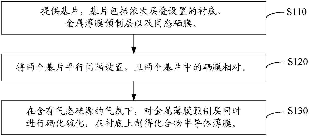
[0034] like figure 1 Shown, the preparation method of the compound semiconductor thin film of one embodiment, comprises the following steps:
[0035] S110, providing a substrate, which includes a substrate, a metal thin film prefabricated layer, and a solid selenium film that are sequentially stacked.
[0036] Please also refer to figure 2 , the substrate includes a substrate 210 and a back electrode layer 220 deposited on the substrate 210 . Firstly, a substrate 210 is provided, and the material of the substrate 210 can be selected from soda lime glass, flexible stainless steel or polyimide plastic. Afterwards, the back electrode layer 220 may be deposited on the substrate 210 by sputtering or vapor deposition. The back electrode layer 220 may be a metal layer such as molybdenum.
[0037] The metal thin film prefabricated layer 230 can be formed on the back electrode layer 220 by an evaporation method or a sputtering method. The metal thin film prefabricated layer 230 m...
Embodiment 1
[0082] A layer of molybdenum was sputtered on a soda-lime glass substrate with a side length of 10cm*10cm as the back electrode layer.
[0083] Using a copper-gallium target with a gallium content of 25 wt%, sputter-deposit a copper-gallium film with a thickness of 250 nm on the molybdenum back electrode, and then use an indium target to continue sputter-depositing an indium film with a thickness of 550 nm to obtain copper indium gallium Prefab layers.
[0084] Then, a solid selenium film with a thickness of 850nm is vapor-deposited on the copper indium gallium prefabricated layer to obtain a substrate, in which the substrate, the back electrode layer, the metal thin film prefabricated layer and the solid selenium film are sequentially stacked.
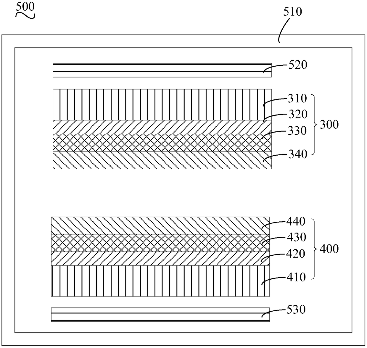
[0085] The two substrates are arranged in parallel and spaced apart, and the selenium films in the two substrates face each other, and the distance between the two substrates is 2mm.
[0086] Put the above-mentioned two substrates ar...
PUM
 Abstract
Description
Claims
Application Information
 - R&D
- Intellectual Property
- Life Sciences
- Materials
- Tech Scout
- Unparalleled Data Quality
- Higher Quality Content
- 60% Fewer Hallucinations
Browse by: Latest US Patents, China's latest patents, Technical Efficacy Thesaurus, Application Domain, Technology Topic, Popular Technical Reports.
© 2025 PatSnap. All rights reserved.Legal|Privacy policy|Modern Slavery Act Transparency Statement|Sitemap|About US| Contact US: help@patsnap.com