Polysilicon thin film fabrication method

a thin film and polysilicon technology, applied in the direction of basic electric elements, electrical equipment, semiconductor devices, etc., can solve the problems of non-uniform characteristics, inability to achieve uniform grain size, and inability to accurately control the growth of grain in two or three dimensions, so as to improve the electrical characteristics of tfts, improve the uniformity of device parts of the drive circuit, and control stably

Active Publication Date: 2007-03-20
NAT TAIWAN UNIV
View PDF1 Cites 58 Cited by
  • Summary
  • Abstract
  • Description
  • Claims
  • Application Information

AI Technical Summary

Benefits of technology

[0011]Another object of the present invention is to provide a polysilicon thin film fabrication method, whereby the crystallization of polysilicon thin film can be controlled to achieve uniform electrical properties, thereby improving the electrical characteristics of TFTs.
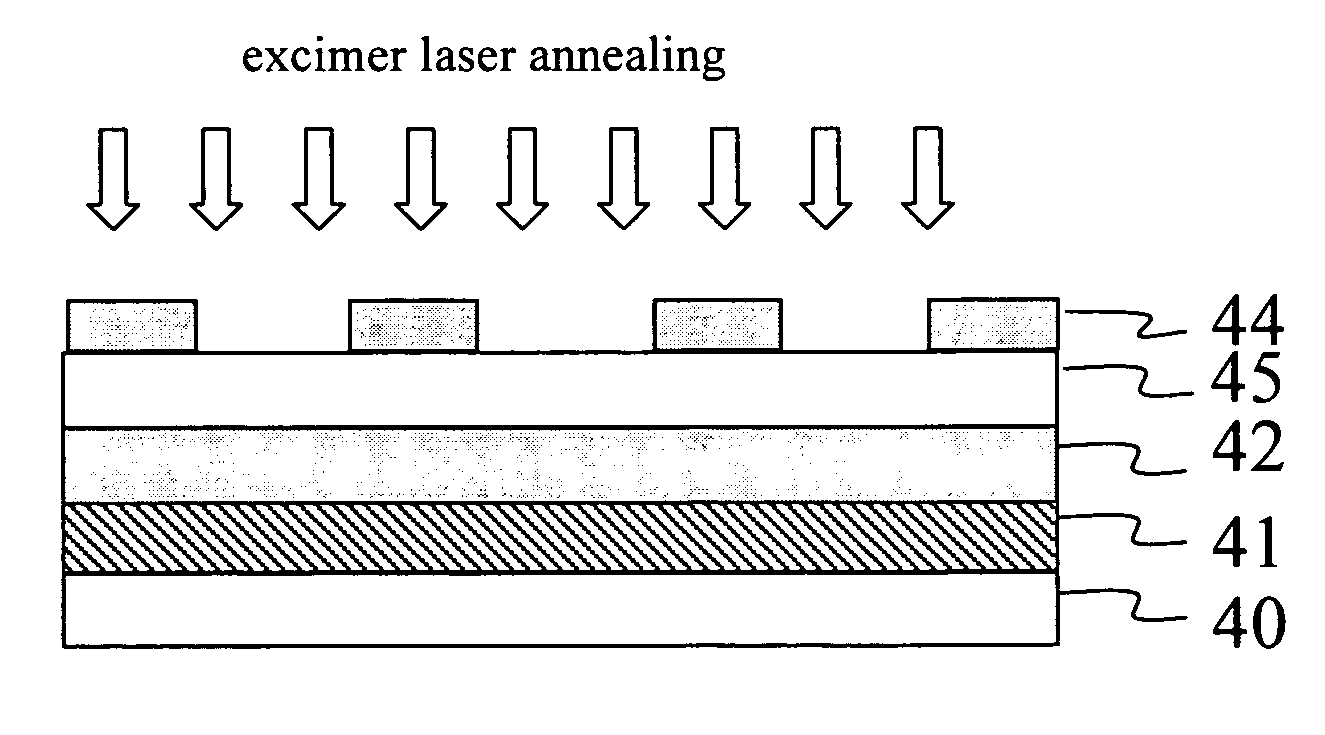
[0012]To achieve the above objects, the present invention proposes a polysilicon thin film fabrication method comprising the steps of: providing a substrate; depositing a heat-absorbing layer on the substrate; depositing an insulating layer on the heat-absorbing layer to block the influence of the heat-absorbing layer to nucleation of Si atoms; depositing an amorphous silicon thin film on the insulating layer; depositing a regular heat-conducting layer as a cooling source on the amorphous silicon thin film; and performing an annealing process to let the amorphous silicon thin film crystallize with the heat-conducting layer as the center and grow outwards to form a uniform polysilicon thin film with regularly arranged grains. Next, the heat-conducting layer can be removed without affecting the electrical properties of the polysilicon thin film. The numbers of grain and grain boundary in the polysilicon thin film channel of the TFT can thus be effectively controlled, and the electrical characteristics of TFTs can also be stably controlled, thereby improving the device uniformity of the whole drive circuit.

Problems solved by technology

Although today's LTPS TFTs have good electrical properties, they have the problem of nonuniform characteristics.
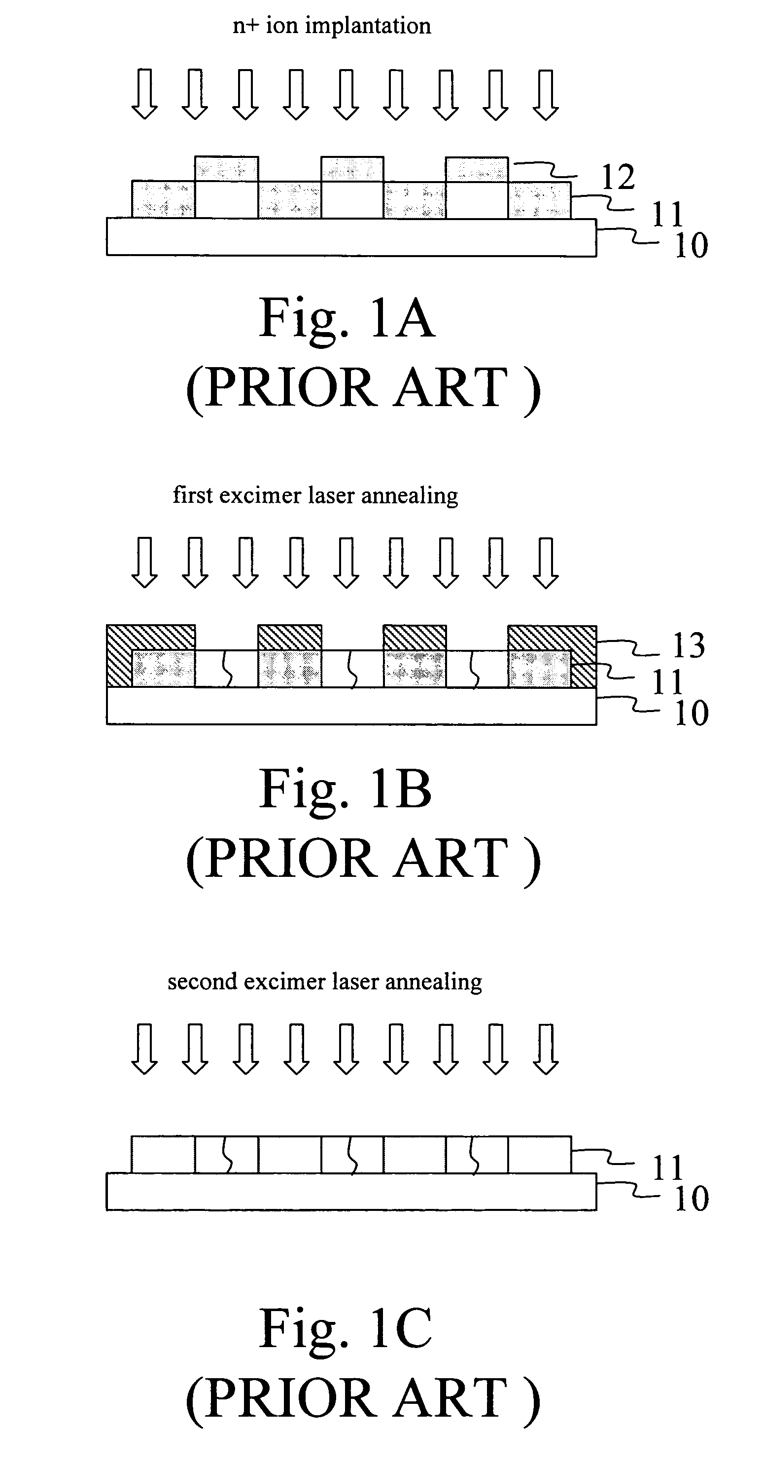
The above method can effectively control the growth of grain in one dimension, but cannot accurately control the growth of grain in two or three dimensions, hence being not able to accomplish uniform grain size.
In other words, the above method cannot control the grain size to achieve uniformity of device.
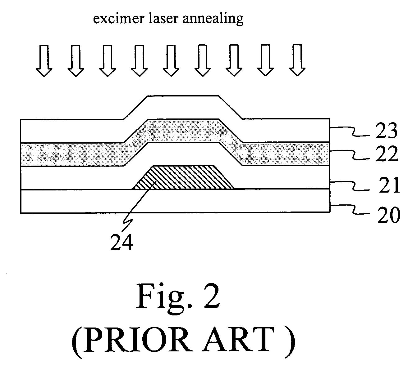
Moreover, different material stresses between thin films may arise during excimer laser annealing due to different thermal expansion coefficients between thin films above the air gap.
Furthermore, because the bottoms of thin films are hollow, crack of thin films may easily occur to affect the stability of the fabrication process.
Although the grain size can reach as high as 10 μm, the uniformity of grain in another direction cannot be controlled.

Method used


Image

  • Polysilicon thin film fabrication method
  • Polysilicon thin film fabrication method
  • Polysilicon thin film fabrication method

Examples


Embodiment Construction

[0020]As shown in FIG. 4, the present invention provides a polysilicon thin film fabrication method, which comprises the following steps.

[0021]First, a substrate is provided (Step S100). The substrate is a glass substrate, an insulator substrate, or a semiconductor substrate. Next, a heat-absorbing layer is formed on the substrate (Step S200). An insulating layer is then formed on the heat-absorbing layer (Step S300). Subsequently, an amorphous silicon thin film is formed on the insulating layer (Step S400). A regular heat-conducting layer is formed on the amorphous silicon thin film (Step S500). Finally, An annealing process is performed to let the amorphous silicon thin film crystallize with the heat-conducting layer as the center and grow outwards to form a uniform polysilicon thin film.

[0022]The present invention will be exemplified below with reference to FIGS. 5A–5H and FIGS. 6A–6C. The polysilicon thin film fabrication method of the present invention comprises the following s...


PUM

PropertyMeasurementUnit
thicknessaaaaaaaaaa
thicknessaaaaaaaaaa
reflectivityaaaaaaaaaa

Abstract

A polysilicon thin film fabrication method is provided, in which a heat-absorbing layer is used to provide sufficient heat for grain growth of an amorphous silicon thin film, and an insulating layer is used to isolate the heat-absorbing layer and the amorphous silicon thin film. A regular heat-conducting layer is used as a cooling source to control the crystallization position and grain size of the amorphous silicon thin film. Therefore, the amorphous silicon thin film can crystallize into a uniform polysilicon thin film, and the electrical characteristics of the polysilicon thin film can be stably controlled.

Description

BACKGROUND OF THE INVENTION[0001]1. Field of the Invention[0002]The present invention relates to a polysilicon thin film fabrication method and, more particularly, to a polysilicon thin film fabrication method capable of enhancing the uniformity of grain.[0003]2. Description of Related Art[0004]The low temperature poly Si (LTPS) thin film transistor (TFT) technology will be used in future active matrix LCDs and OLEDs. Although today's LTPS TFTs have good electrical properties, they have the problem of nonuniform characteristics. In order to improve the nonuniform situation of polysilicon thin film between channels, it is necessary to control the size and distributed distance of polysilicon grains.[0005]In 2000, Seoul University of South Korea has proposed a polysilicon thin film fabrication method, in which the high reflectivity of aluminum is used as a metallic cooling source for sideward growth. As shown in FIGS. 1A–1C, an amorphous silicon thin film 11 of a thickness of 80 nm is ...

Claims


Application Information

Patent Timeline
Patent Type & Authority Patents(United States)
IPC IPC(8): H01L21/00H01L21/20H01L21/336
CPCH01L21/2026H01L27/1296H01L27/1281H01L29/04H01L21/0262H01L21/02667H01L21/02686H01L21/02488H01L21/02502H01L21/02422H01L21/02532
Inventor LEE, SI-CHENMENG, CHAO-YUCHANG, HSU-YU
Owner NAT TAIWAN UNIV
Why Eureka
Try Eureka