NAND flash memory management method, host, NAND flash memory reading and writing method, and NAND flash memory controller

A flash memory management and flash memory technology, which is applied in the direction of instruments, electrical digital data processing, data processing input/output process, etc., can solve the problem of unusable physical blocks and achieve the effect of increasing the available capacity

Inactive Publication Date: 2017-02-22
SHENZHEN CHIPSBANK TECH
View PDF4 Cites 13 Cited by
  • Summary
  • Abstract
  • Description
  • Claims
  • Application Information

AI Technical Summary

Problems solved by technology

[0005] Embodiments of the present invention provide a NAND flash memory management method, a host, a NAND flash memory read and write method, and a NAND flash memory controller, which are used to solve the problem of binding good physical blocks and bad physical blocks together in the prior art, resulting in the entire The problem that the bound physical block cannot be used

Method used


Image

  • NAND flash memory management method, host, NAND flash memory reading and writing method, and NAND flash memory controller
  • NAND flash memory management method, host, NAND flash memory reading and writing method, and NAND flash memory controller
  • NAND flash memory management method, host, NAND flash memory reading and writing method, and NAND flash memory controller

Examples


Embodiment Construction

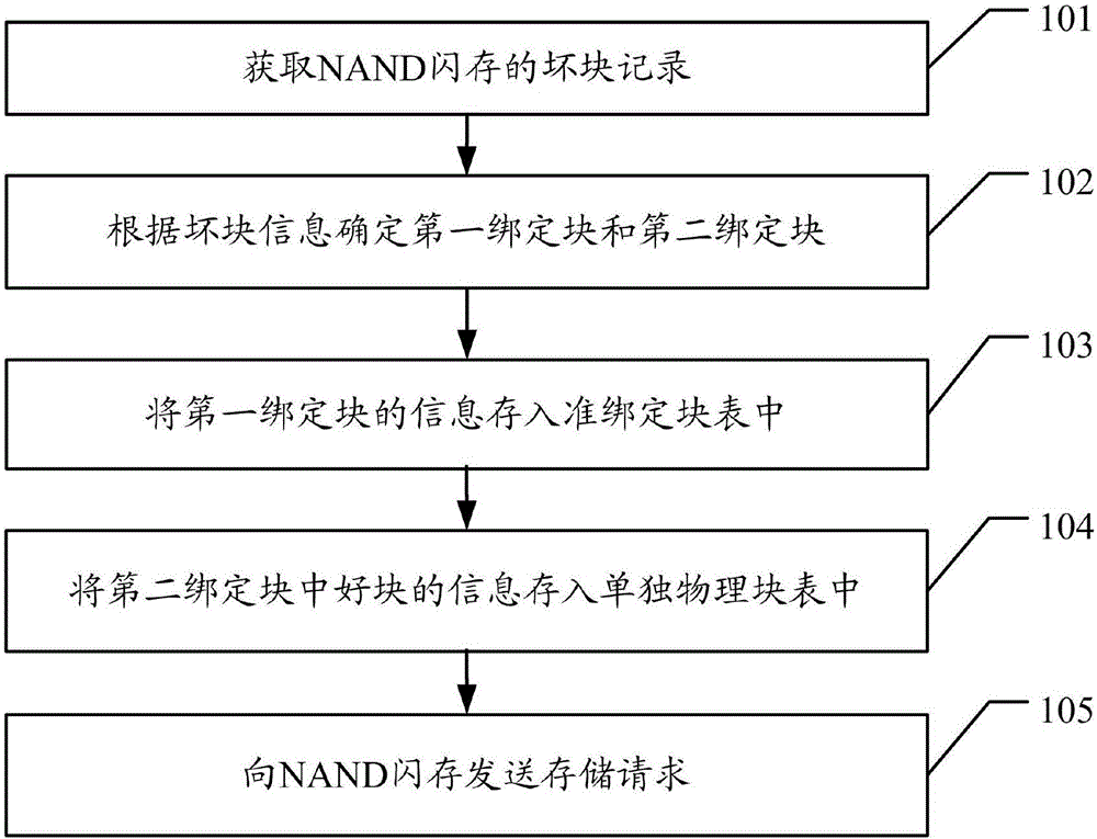
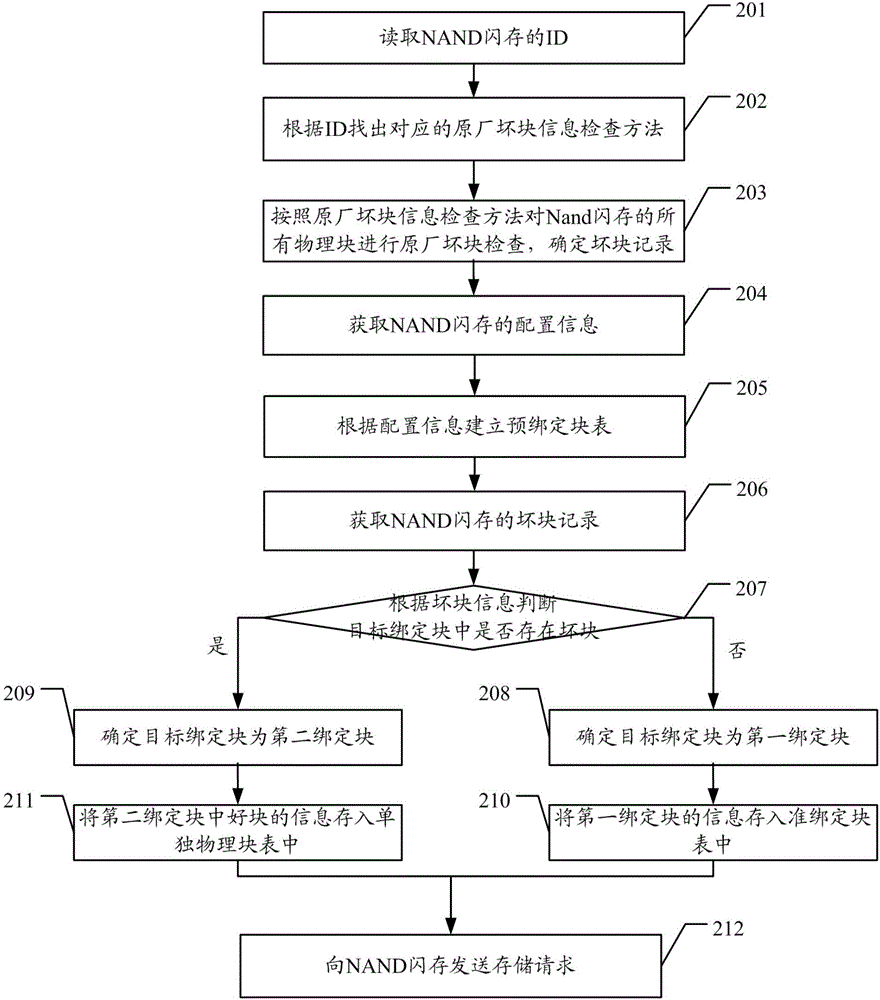
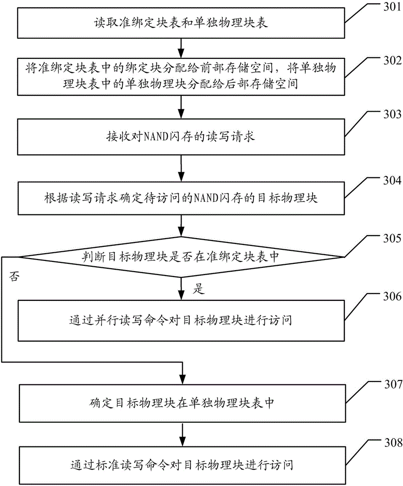
[0056] Embodiments of the present invention provide a NAND flash memory management method, a host computer, a NAND flash memory reading and writing method, and a NAND flash memory controller, which are used to increase the available capacity of the NAND flash memory on the premise of ensuring a high access speed of the NAND flash memory.

[0057] In order to enable those skilled in the art to better understand the solutions of the present invention, the following will clearly and completely describe the technical solutions in the embodiments of the present invention in conjunction with the drawings in the embodiments of the present invention. Obviously, the described embodiments are only It is an embodiment of a part of the present invention, but not all embodiments. Based on the embodiments of the present invention, all other embodiments obtained by persons of ordinary skill in the art without making creative efforts shall fall within the protection scope of the present invent...


PUM


Abstract

The embodiment of the invention discloses an NAND flash memory management method, a host, an NAND flash memory reading and writing method, and an NAND flash memory controller. The NAND flash memory management method provided by the embodiment of the invention comprises the steps of acquiring bad block information of an NAND flash memory; determining a first binding block and a second binding block according to the bad block information, wherein mutually bound physical blocks in the first binding block are all good blocks, and mutually bound physical blocks in the second binding block comprise bad blocks; storing the information of the first binding block into a future binding block list, and storing the information of the good blocks in the second binding block into an independent physical block list in the NAND flash memory; and sending a storage request to the NAND flash memory, wherein the storage request comprises the future binding block list and the independent physical block list, thus allowing the NAND flash memory controller to store the future binding block list and the independent physical block list into the NAND flash memory, access the first binding block via a parallel reading-writing command, and access the good blocks in the second binding block via a standard reading-writing command. According to the method provided by the invention, both high speed and high capacity of the NAND flash memory can be achieved.

Description

technical field [0001] The invention relates to the technical field of data storage, in particular to a NAND flash memory management method, a host computer, a NAND flash memory reading and writing method, and a NAND flash memory controller. Background technique [0002] With the popularity of various mobile electronic devices, storage devices using NAND flash media as data storage media have become more popular and widely used, which has led to a substantial increase in the required capacity. Based on the existing NAND flash memory models The method to increase the capacity is to connect multiple NAND flash memories of the same type in series and parallel to increase the capacity. The importance of speed has come to the fore as capacity has increased. [0003] In the traditional technology, when accessing the flash memory, for example, when two pages of data need to be written, the second page of data needs to be written after the first page of data is written, which requi...

Claims


Application Information

Patent Timeline
Patent Type & Authority Applications(China)
IPC IPC(8): G06F3/06
CPCG06F3/0617G06F3/064G06F3/0679
Inventor 陈伟
Owner SHENZHEN CHIPSBANK TECH
Why Eureka
Try Eureka