MEMS microphone encapsulation

A microphone and ASIC chip technology, applied in the field of acoustic and electrical products, can solve the problems of high electrical signal transmission consumption, poor product reliability, electrical signal distortion, etc., and achieve the effects of low transmission consumption, low production cost, and improved performance and reliability.

Active Publication Date: 2017-02-22
WUXI RED MICROELECTRONICS CORP
View PDF5 Cites 1 Cited by
  • Summary
  • Abstract
  • Description
  • Claims
  • Application Information

AI Technical Summary

Problems solved by technology

[0003] The schematic diagram of the existing MEMS microphone PCB board in the prior art is as follows figure 1 As shown, the PCB board is provided with a connected MEMS chip 2 and an ASIC (application specific integrated circuit) chip 3, and the output port, GND port, and VDD port of the ASIC chip are respectively connected to the front pad 13 of the PCB board, and the front pad passes through The copper layer 14 set in the PCB is connected to the back pad 11 of the PCB board and then connected to external components. However, such a package structure conducts electrical signals through the copper layer in the PCB. In actual use, the consumption of electrical signal transmission is relatively large and the signal is affected Large interference will cause electrical signal distortion, huge heat generation and other disadvantages, and the product reliability is poor

Method used


Image

  • MEMS microphone encapsulation
  • MEMS microphone encapsulation

Examples


Embodiment Construction

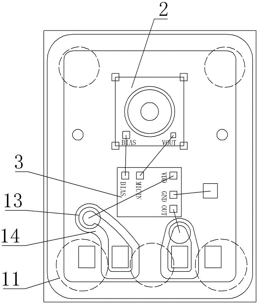
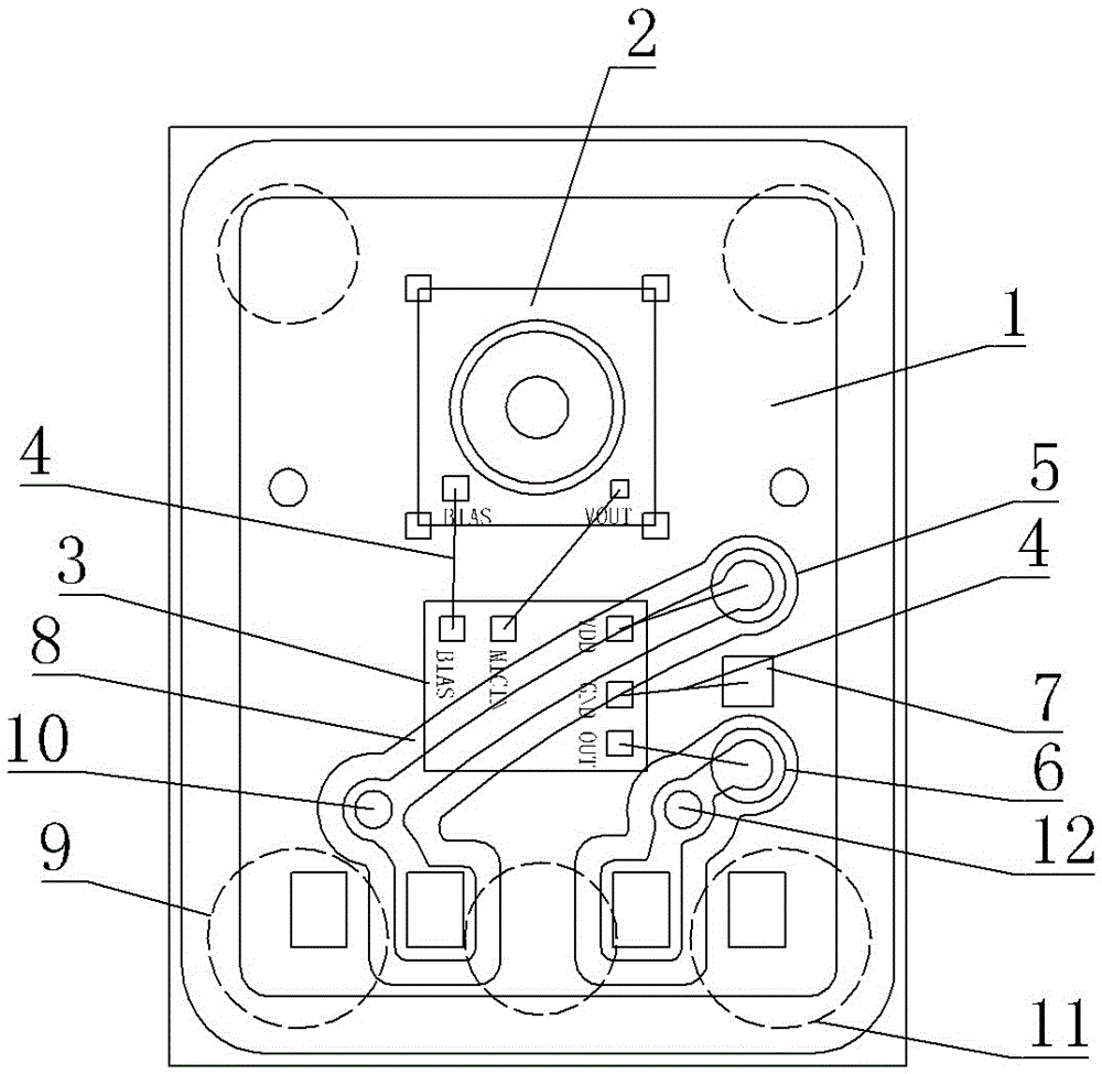
[0014] See figure 2 , a MEMS microphone package, including an upper PCB board 1 and a lower PCB board, the upper PCB board 1 is provided with a MEMS chip 2 and an ASIC chip 3, the ASIC chip is NJU72082G, the MEMS chip is NJD3005e, and the BIAS of the MEMS chip 2 The port is connected to the BIAS port of the ASIC chip 3 through a gold wire 4, the VOUT port of the MEMS chip 2 is connected to the MICIN port of the ASIC chip 3 through a gold wire, and the VDD port of the ASIC chip 3 is connected to the VDD soldering port on the front side of the upper PCB board 1 through a gold wire. Disk 5, the OUT port of the ASIC chip 3 is connected to the output pad 6 arranged on the front of the upper PCB board 1 through a gold wire, and the GND port of the ASIC chip 3 is connected to the ground pad 7 arranged on the front of the upper PCB board 1 through a gold wire. The first copper layer 8 and the second copper layer 9 are arranged between the PCB 1 and the lower PCB, and the VDD pad 5 is...


PUM


Abstract

The invention provides MEMS microphone encapsulation. The structure is simple; a universal MEMS chip and ASIC chip are adopted; the encapsulation cost is not increased; therefore, electrical signal transmission loss and interference are reduced to be minimal; the transmission performance is good; the electrical signal transmission reliability is ensured; an upper PCB and a lower PCB are included; the MEMS chip and the ASIC chip are arranged on the upper PCB; the MEMS chip and the ASIC chip are connected through a conductor wire; the ASIC chip is connectedly arranged on an upper bonding pad on the upper PCB through the conductor wire; a copper layer is arranged between the upper PCB and the lower PCB; the MEMS microphone encapsulation is characterized in that through holes are respectively arranged, and sequentially pass through the upper PCB, the copper layer and the lower PCB; and the through holes are connected with the back bonding pad arranged at the back of the lower PCB.

Description

technical field [0001] The invention relates to the technical field of acoustic and electric products, in particular to a MEMS microphone package. Background technique [0002] With the rapid development of electronic technology, MEMS (micro-electro-mechanical systems) microphones have gained popularity due to their advantages of small size, easy SMT (surface mount technology) installation, high temperature resistance, good stability, high degree of automation and suitable for mass production. more and more widely used. [0003] The schematic diagram of the existing MEMS microphone PCB board in the prior art is as follows figure 1 As shown, the PCB board is provided with a connected MEMS chip 2 and an ASIC (application specific integrated circuit) chip 3, and the output port, GND port, and VDD port of the ASIC chip are respectively connected to the front pad 13 of the PCB board, and the front pad passes through The copper layer 14 set in the PCB is connected to the back pa...

Claims


Application Information

Patent Timeline
Patent Type & Authority Applications(China)
IPC IPC(8): H04R19/04
CPCH04R19/04H04R2400/11
Inventor 王志超
Owner WUXI RED MICROELECTRONICS CORP
Why Eureka
Try Eureka