tsop package lead frame anti-delamination structure
A technology of encapsulating leads and layered structure, which is applied in the direction of semiconductor/solid-state device components, semiconductor devices, electrical components, etc., can solve problems such as product reliability, poor shrinkage force, and poor stress resistance, and achieve vacuum protection Effects of fixing, reducing possibility, increasing punching area
- Summary
- Abstract
- Description
- Claims
- Application Information
AI Technical Summary
Problems solved by technology
Method used
Image

Examples
Embodiment Construction
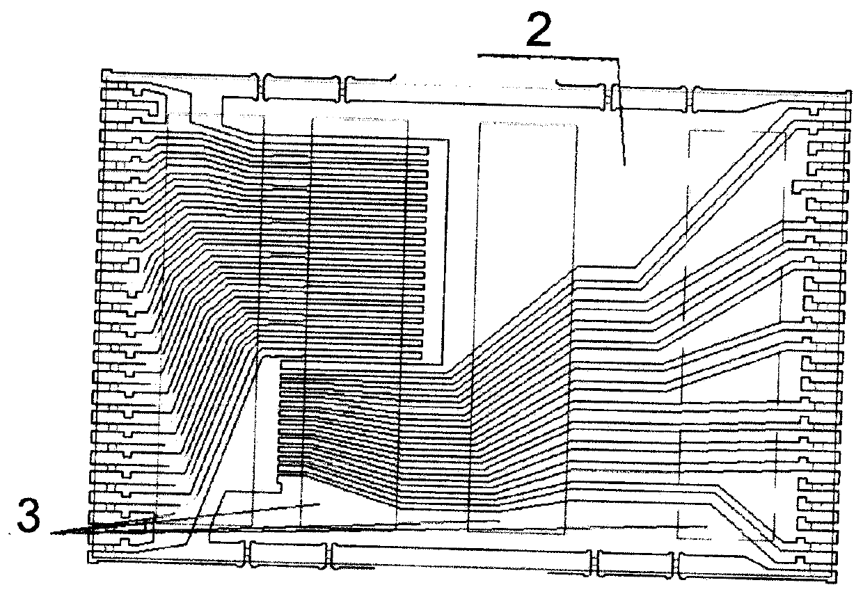
[0014] Such as figure 1 with figure 2 As shown, the comparison between the anti-layered structure of the lead frame of the TSOP package of the present invention and the existing layered structure lies in the fact that the large copper area of the existing layered structure (such as figure 1 (Shown), it can be well absorbed by the wire bonding machine suction plate, but it will cause the problem of injection delamination. After injection molding, there is less communication between the resin surfaces, and the area of the bonding surface with the lead frame is relatively large, resulting in two independent The body has a large stress difference due to different shrinkage rates, resulting in delamination (such as figure 2 Shown).
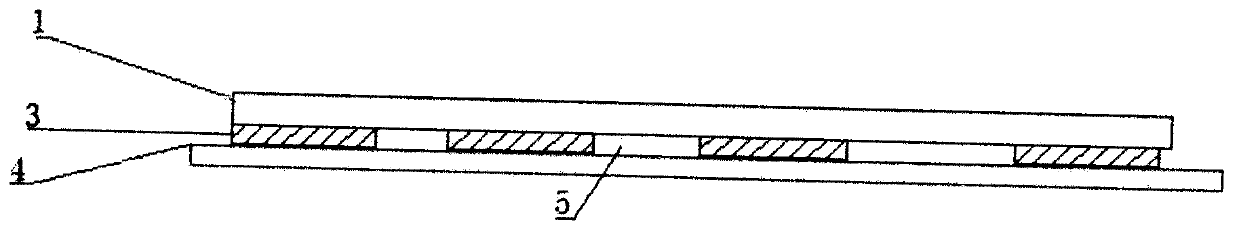
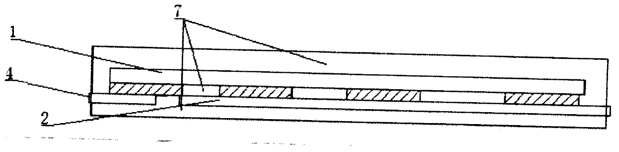
[0015] Such as image 3 with Figure 4 As shown, the anti-layered structure of the TSOP package lead frame of the present invention includes a wafer IC1, tape 3, a lead frame 4 and a floating area 5. A large area copper area 2 is provided on the lead...
PUM
 Abstract
Description
Claims
Application Information