MOS tube parameter degradation circuit, test circuit and early warning circuit

A MOS tube and parameter degradation technology, applied in the field of monitoring, can solve the problems of reduced output signal accuracy, MOS tube failure, and inaccurate test results.

Active Publication Date: 2017-03-22
CHINA ELECTRONICS PROD RELIABILITY & ENVIRONMENTAL TESTING RES INST
View PDF6 Cites 9 Cited by
  • Summary
  • Abstract
  • Description
  • Claims
  • Application Information

AI Technical Summary

Problems solved by technology

[0003] As mentioned above, the HCI effect will cause changes in the parameters of the MOS tube. In particular, when the threshold voltage and transconductance degradation exceed a certain limit due to the accumulation of charge in the gate oxide layer, the MOS tube will fail.
Therefore, the hot carrier injection effect is an important factor affecting the performance parameters of MOS tubes, and it is also one of the failure mechanisms that lead to high device failure rates.
[0004] At this stage, in the MOS tube parameter degradation circuit caused by the HCI effect, due to the HCI effect, NBTI (Negative Bias Temperature Instability, negative bias temperature instability) effect and TDDB (time dependent dielectric breakdown, and Time-related dielectric breakdown) effects and other factors, so the output signal of the above-mentioned MOS tube parameter degradation circuit will be affected by various effects, reducing the accuracy of the output signal
When testing the output signal of the MOS tube parameter degradation circuit, the test results will not be accurate, so that it is impossible to accurately warn the MOS tube failure caused by the HCI effect

Method used


Image

  • MOS tube parameter degradation circuit, test circuit and early warning circuit
  • MOS tube parameter degradation circuit, test circuit and early warning circuit
  • MOS tube parameter degradation circuit, test circuit and early warning circuit

Examples


Embodiment Construction

[0058] In order to further explain the technical means adopted by the present invention and the effects obtained, the technical solutions of the embodiments of the present invention will be clearly and completely described below in conjunction with the accompanying drawings and preferred embodiments.

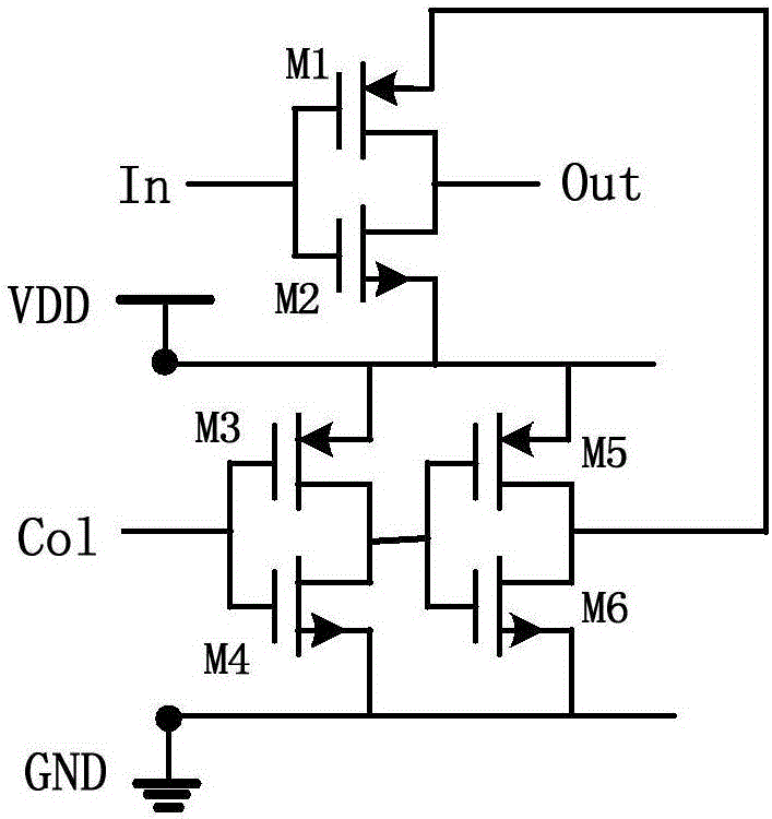
[0059] See figure 1 with figure 2 , a MOS transistor parameter degradation circuit, comprising an NMOS transistor M1 and a PMOS transistor M2; the gate of the NMOS transistor M1 is connected to the gate of the PMOS transistor M2, and the drain of the NMOS transistor M1 is connected to the PMOS transistor The drain of M2 is connected; the gate of the PMOS transistor M2 is connected to the power supply VDD; the source of the NMOS transistor M1 receives the control signal Col, and the control signal Col adopts a level signal. When the control signal Col is a high-level signal, the channel of the NMOS transistor M1 generates hot carriers; wherein, the process of injecting the hot ...


PUM


Abstract

The invention relates to an MOS tube parameter degradation circuit comprising an NMOS tube and a PMOS tube, wherein the grid of the NMOS tube is connected with the grid of the PMOS tube, and the drain electrode of the NMOS tube is connected with the drain electrode of the PMOS tube; the grid of the PMOS tube is connected with a power supply; the source electrode of the NMOS tube receives a control signal; when the control signal is a high-level signal, a channel of the NMOS tube generates hot carriers; and the grid of the NMOS tube and the grid of the PMOS tube receive input signals, and the drain electrode of the NMOS tube and the drain electrode of the PMOS tube output inverted output signals of the input signals. The MOS tube parameter degradation circuit can improve the accuracy of the output signals. The invention further relates to an MOS tube parameter degradation test circuit capable of improving the accuracy of a test result, another MOS tube parameter degradation test circuit capable of improving the accuracy of the test result, an MOS tube parameter degradation early warning circuit capable of performing accurate early warning and another MOS tube parameter degradation early warning circuit capable of performing accurate early warning.

Description

technical field [0001] The present invention relates to the technical field of monitoring, in particular to a MOS tube parameter degradation circuit, a MOS tube parameter degradation test circuit, another MOS tube parameter degradation test circuit, a MOS tube parameter degradation early warning circuit, and another MOS tube parameter degradation warning circuit. Background technique [0002] With the development of ultra-large-scale integrated circuit manufacturing technology towards the nanometer direction, the size of each device of the integrated circuit is reduced accordingly. Correspondingly, the MOS transistor (metal oxide semiconductor, metal-oxide-semiconductor field effect transistor) , and its feature size is getting smaller and smaller, but the normal operating voltage of the MOS tube has not been reduced proportionally, which will cause the local electric field inside the MOS tube channel to become larger and larger. With the increase of the local electric fiel...

Claims


Application Information

Patent Timeline
Patent Type & Authority Applications(China)
IPC IPC(8): H03K17/16G01R31/26
CPCG01R31/2621H03K17/16
Inventor 雷登云恩云飞陈义强何春华黄云
Owner CHINA ELECTRONICS PROD RELIABILITY & ENVIRONMENTAL TESTING RES INST
Why Eureka
Try Eureka