Preparation technology of high-hardness anti-fingerprint ultra-narrow border mobile phone touch screen
A preparation process and anti-fingerprint technology, applied in equipment with touch panel/sensor/detector, input/output process of data processing, instruments, etc., can solve the problems of touch screen easy to scratch, fingerprint pollution, etc., and achieve good durability Effects of friction performance, low cost, and simple manufacturing method
- Summary
- Abstract
- Description
- Claims
- Application Information
AI Technical Summary
Problems solved by technology
Method used
Image
Examples
specific Embodiment approach 1
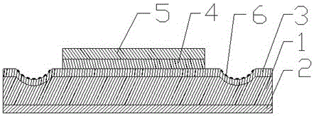
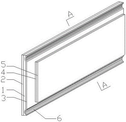
[0043] Specific implementation mode 1: In this implementation mode, the manufacturing process of the high-hardness anti-fingerprint ultra-narrow frame mobile phone touch screen is realized according to the following steps:
[0044] Step 1. Glass substrate 1 processing
[0045] Prepare the glass substrate 1, process two semicircular grooves equal to the length of the glass substrate 1 on the upper surface of the glass substrate 1; the grooves are parallel to the length direction of the glass substrate 1, and the two grooves are respectively arranged on the glass substrate Edges on both sides of the upper surface;
[0046] Step 2, preparing the first ITO conductive layer 2
[0047] Coating the first ITO conductive layer 3 on the lower surface of the glass substrate 1;
[0048] Step 3, preparing the second ITO conductive layer 3
[0049] Coating a second ITO conductive layer 3 on the upper surface of the glass substrate 1 and the upper surface of the groove;
[0050] Step 4. ...
specific Embodiment approach 2
[0061] Embodiment 2: This embodiment differs from Embodiment 1 in that: the glass substrate 1 in step 1 is a tempered glass substrate, strengthened glass substrate, common glass substrate or a transparent polymer material substrate. Other steps and parameters are the same as those in the first embodiment.
specific Embodiment approach 3
[0062] Embodiment 3: The difference between this embodiment and Embodiment 1 or 2 is that the electronic circuit 6 in Step 5 is made of carbon paste or silver paste. Other steps and parameters are the same as those in Embodiment 1 or 2.
PUM
| Property | Measurement | Unit |
|---|---|---|
| thickness | aaaaa | aaaaa |
| thickness | aaaaa | aaaaa |
Abstract
Description
Claims
Application Information

