A method of improving the performance of flash memory chip

A flash memory chip and performance technology, applied in the field of memory, can solve the problems of memory cell missearch, failure, and chip cannot be repaired normally, and achieve the effect of eliminating missearch, improving performance, and preventing chips from failing to repair normally.

Active Publication Date: 2019-12-31
WUHAN XINXIN SEMICON MFG CO LTD
View PDF6 Cites 0 Cited by
  • Summary
  • Abstract
  • Description
  • Claims
  • Application Information

AI Technical Summary

Problems solved by technology

Due to the presence of a single or a few slow-erasing memory cells in the array area, firstly, during the performance test, the erasure time of the chip or sector will exceed the specified time and cause failure; secondly, the entire sector will be invalid during the test. The erasing time is getting longer and longer. As the test progresses, the erasing time may be several times or even dozens of times that of the normal sector, resulting in the performance of the flash memory chip failing to meet customer requirements
[0004] At present, flash memory chips search for memory cells that are slowly erased mainly through a uniform and fixed reference current or reference voltage to find problems in the form of read operations, which will cause the following problems: all memory cells that are slowly erased cannot be searched To; the normal memory unit is mistakenly searched, and too many false searches will cause too many memory cells to be repaired, resulting in the failure of the chip to be repaired normally

Method used


Image

  • A method of improving the performance of flash memory chip
  • A method of improving the performance of flash memory chip
  • A method of improving the performance of flash memory chip

Examples


Embodiment Construction

[0033] The present invention will be further described below in conjunction with the accompanying drawings and embodiments.

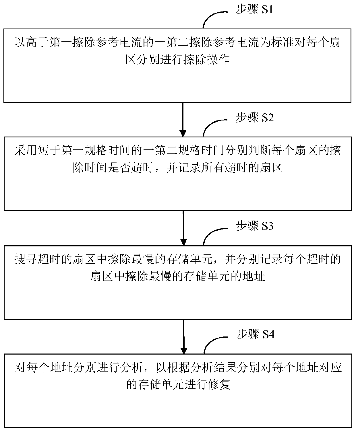
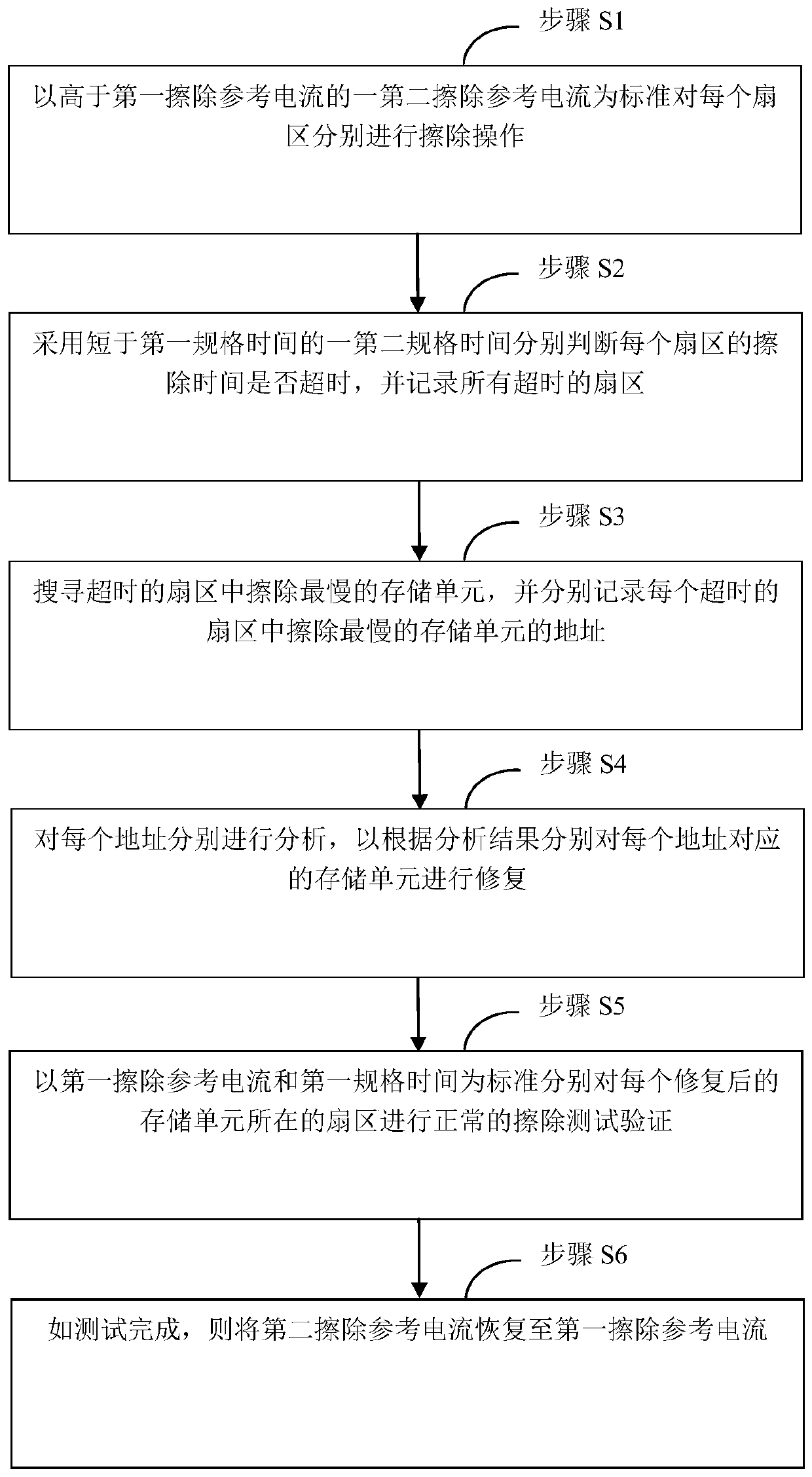
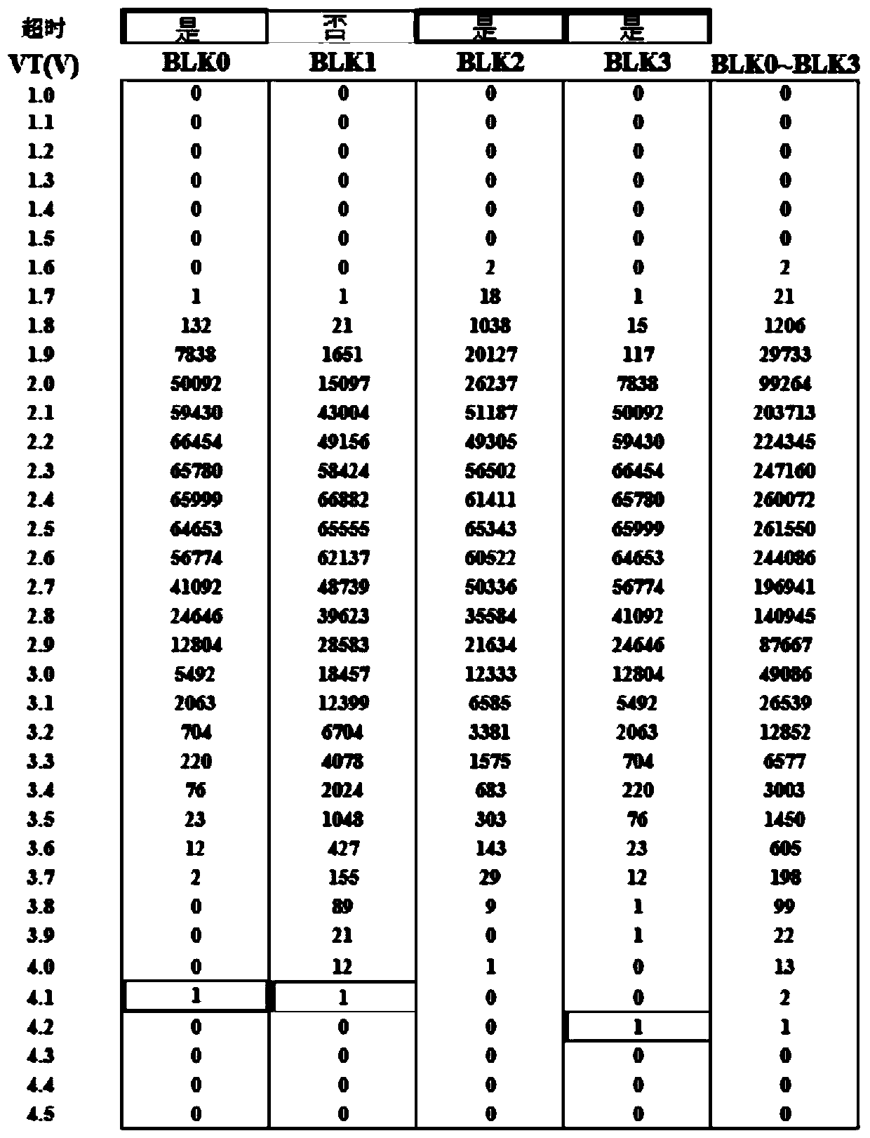
[0034] In a preferred embodiment, as figure 1 As shown, a method for improving the performance of the flash memory chip is proposed, the flash memory chip includes a storage array, the storage array includes a plurality of sectors, each sector includes a plurality of storage units, and each storage unit is used to preserve one bit of data;

[0035] providing a first erasing reference current for comparing with the current in the memory unit to determine whether the data stored in the memory unit is erased;

[0036] Provide a first specification time for judging whether the sector expires in the erasing process;

[0037] Methods also include:

[0038] Step S1, performing an erasing operation on each sector with a second erasing reference current higher than the first erasing reference current as the standard;

[0039] Step S2, using a second specifica...


PUM


Abstract

The present invention relates to the field of memory, in particular to a method for improving the performance of a flash memory chip, comprising: performing an erasing operation on each sector based on a second erasing reference current; Whether the erasing time of each sector is overtime, and record all overtimed sectors; search for the slowest erasing storage unit in the overtimed sector, and record the slowest erasing storage unit in each overtimed sector address; each address is analyzed separately to repair the memory cells corresponding to each address according to the analysis results; the above technical solution increases the standard first erasing reference current to hide deeper erasing slow The storage unit is exposed, and at the same time, false search for normal storage units can be eliminated, thereby avoiding the problem that the chip cannot be normally repaired due to too many storage units to be repaired due to this problem.

Description

technical field [0001] The invention relates to the field of memory, in particular to a method for improving the performance of a flash memory chip. Background technique [0002] A flash memory chip generally includes an array area formed by storage devices distributed in an array, each storage unit is used to store one bit of data, and the storage units in the array area are usually logically divided to form a plurality of sectors. [0003] The market is increasingly demanding the speed and performance of erase operations for flash memory products. Due to the presence of a single or a few slow-erasing memory cells in the array area, firstly, during the performance test, the erasure time of the chip or sector will exceed the specified time and cause failure; secondly, the entire sector will be invalid during the test. The erasing time is getting longer and longer. As the test progresses, the erasing time may be several times or even dozens of times that of the normal sector...

Claims


Application Information

Patent Timeline
Patent Type & Authority Patents(China)
IPC IPC(8): G11C29/44G11C29/50
CPCG11C29/44G11C29/50G11C2029/5004G11C2029/5006
Inventor 陆磊周第廷
Owner WUHAN XINXIN SEMICON MFG CO LTD
Why Eureka
Try Eureka