Method and apparatus for generating temperature-compensated read and verify operations in flash memories

a flash memory and temperature-compensated technology, applied in the field of non-volatile semiconductor memories, can solve the problems of reducing the margin available for distinguishing between programmed and unprogrammed flash cells, and the current characteristics of flash cells may change with changes, so as to achieve the effect of increasing the verification margin

Active Publication Date: 2007-10-02
MICRON TECH INC
View PDF45 Cites 109 Cited by
  • Summary
  • Abstract
  • Description
  • Claims
  • Application Information

AI Technical Summary

Problems solved by technology

However, the current characteristics of a flash cell may change with changes in temperature.
This temperature change may reduce the margin available for distinguishing between a programmed and unprogrammed flash cell.

Method used


Image

  • Method and apparatus for generating temperature-compensated read and verify operations in flash memories
  • Method and apparatus for generating temperature-compensated read and verify operations in flash memories
  • Method and apparatus for generating temperature-compensated read and verify operations in flash memories

Examples


Embodiment Construction

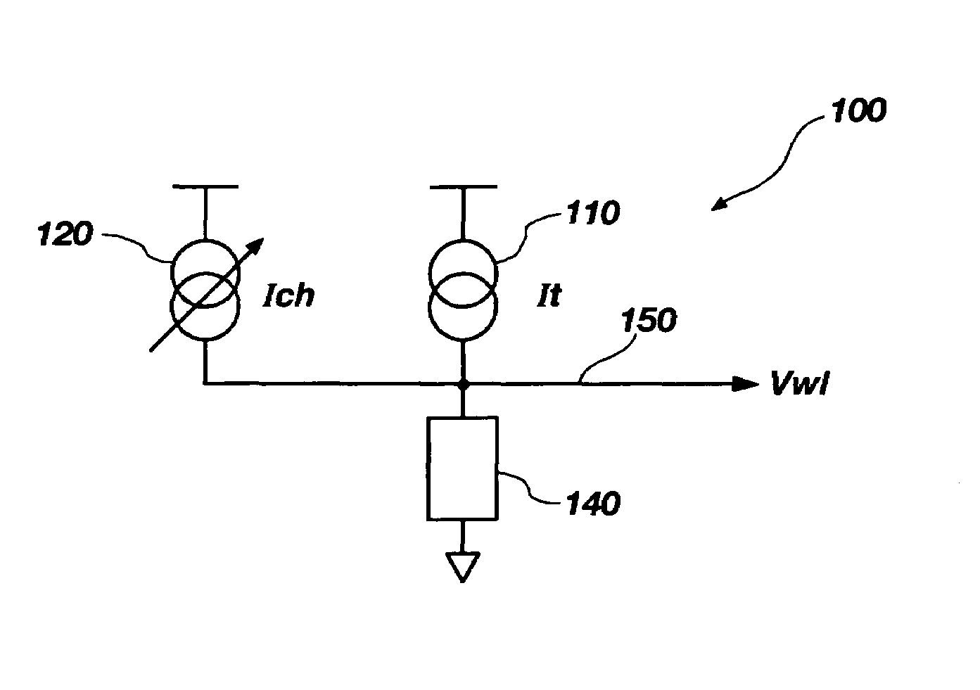
[0034]Some circuits in this description may contain a well-known circuit configuration known as a diode-connected transistor. A diode-connected transistor is formed when the gate and drain of a Complementary Metal Oxide Semiconductor (CMOS) transistor are connected together, or when the base and collector of a bipolar transistor are connected together. When connected in this fashion the transistor operates with voltage to current properties similar to a P-N junction diode. Accordingly, circuit elements illustrated in the figures as diodes may be embodied in any device creating a P-N junction with diode characteristics, such as, for example, a conventional diode, a bipolar transistor connected in a diode configuration, or a CMOS device connected in a diode configuration. Furthermore, suitable devices with diode characteristics may be referred to as diodes, P-N junction elements, diode-connected CMOS transistors, and diode connected bipolar transistor.

[0035]The description herein may ...


PUM


Abstract

Methods and an apparatuses for generating a word-line voltage are disclosed. A word-line voltage generator includes a first current source, an adjustable current source, adjustable current sink, and a voltage converter, all operably coupled to a current sum node. The first current source generates a first current having a temperature coefficient substantially equal to a temperature coefficient of at least one bit cell. The adjustable current source generates a second current that is substantially independent of a temperature change. The adjustable current sink sinks a third current that is substantially independent of a temperature change. The voltage converter is configured for generating a word-line signal having a word-line voltage proportional to a reference current, wherein the reference current comprises the first current, plus the second current, and minus the third current.

Description

BACKGROUND OF THE INVENTION[0001]1. Field of the Invention[0002]The present invention relates to non-volatile semiconductor memories. More specifically, the present invention relates to compensating for temperature variations that may occur during operation of the semiconductor memories.[0003]2. Description of Related Art[0004]Non-volatile semiconductor memories are becoming increasingly popular in a wide range of electronic applications from computer systems to personal appliances such as cellular phones, personal digital assistants, cameras, and music players. With the increased popularity, comes increased need for placing larger volumes of data on an individual device and operating the devices with lower power consumption.[0005]Non-volatile memory cells, such as Electrically Erasable Programmable Memories (EEPROMS) and Flash EEPROMS, store information in a field effect transistor (FET) using a floating gate disposed between the substrate and a control gate. FIG. 1 illustrates a f...

Claims


Application Information

Patent Timeline
Patent Type & Authority Patents(United States)
IPC IPC(8): G11C8/00G11C11/34
CPCG11C5/14G11C7/04G11C16/30G11C16/08G11C8/08
Inventor TANZAWA, TORU
Owner MICRON TECH INC
Why Eureka
Try Eureka