Semiconductor memory device

a memory device and semiconductor technology, applied in the field of semiconductor memory devices, can solve the problems of changing the data holding characteristic of the memory cell, and reducing the threshold voltag

Inactive Publication Date: 2004-10-19
RENESAS ELECTRONICS CORP
View PDF3 Cites 119 Cited by
  • Summary
  • Abstract
  • Description
  • Claims
  • Application Information

AI Technical Summary

Problems solved by technology

Therefore, if writing / erasing are repeatedly performed, an insulating film in an electron accumulating region or in an electron passing-through region would be deteriorated, to cause a problem of a change in data holding characteristic of a memory cell.
An excessively decreased threshold voltage in erasure reduces the threshold voltage after writing by the excessively decreased amount.
Furthermore, in a case of the leakage of electrons, electrons would be trapped in an oxide film to reduce the a voltage applied on a control gate in writing effectively, and a sufficient electric field is not applied between a nitride film and a substrate region, to hinder accumulation of a sufficient amount of electrons in the charge accumulation.
As the second, electrons are continuously kept being trapped in an oxide film and electrons can not be extracted from the nitride film sufficiently.
Therefore, read failure is likely to occur due to margin shortage when a window of verify voltages is shifted in common to all the memory cells.
Therefore, characteristics of all of the memory cells in the non-volatile semiconductor memory device are set according to the worst memory cell characteristic, resulting in promotion of deterioration in characteristics of memory cells as a whole.
Therefore, an amount of shift would be varied even by application of the same rewrite pulse, and therefore, desired threshold voltage shift could not be provided correctly at all times.
In a case where a plural kinds of such reference memory transistors are provided outside the memory cell array and have the respective threshold voltages adjusted in accordance with an operation mode, the control becomes complex.
In addition, it is very difficult to form memory cell transistors the same in characteristic as memory cell transistors outside the memory cell array.
The above problem also similarly arises in a case where read voltage Vread is set to a level higher than a threshold voltage of a memory cell in written state and a difference between currents of the memory cells in written state and in erase state is utilized.
In such a construction, when the reference current is shifted toward a higher level, a difference between a memory cell current flowing in a memory cell in the written state and the reference current becomes smaller, and correct reading of data could not be achieved.
Therefore, a difference MGA between comparison reference current Iref and residual current Irmn (P) is reduced, and a sense margin is smaller, leading to a possibility of occurrence of incorrect reading.
Similarly, in a case where a threshold voltage is raised, if the comparison reference current Iref is increased for all the memory cells commonly, a margin for residual current Irmn(P) of a memory cell in a high threshold voltage state is reduced smaller, leading to a possibility to produce a wrong reading.
When internal read data of sense amplifier 3 is defective, it is determined that a margin failure is brought about, to change a set condition for reference current for a memory cell with the margin failure.
In data reading, when a margin failure is further detected at a registered address, a prescribed error processing is performed.
In such low threshold voltage state, a state likely to cause a margin failure is the state in which the threshold voltage is shifted to a higher level.
In an erase operation, the reference current condition is changed when a predetermined number of times of verification is performed and a verify defect occurs in the verify operation of a memory cell.
In step S61, however, if the main sense result and the sub sense result are in coincidence with each other, but the main sense result is different from rewrite data in logical level, necessary error processing is performed, based on the determination that a rewrite defect occurs and a margin failure is not resolved yet.

Method used


Image

  • Semiconductor memory device
  • Semiconductor memory device
  • Semiconductor memory device

Examples


second embodiment

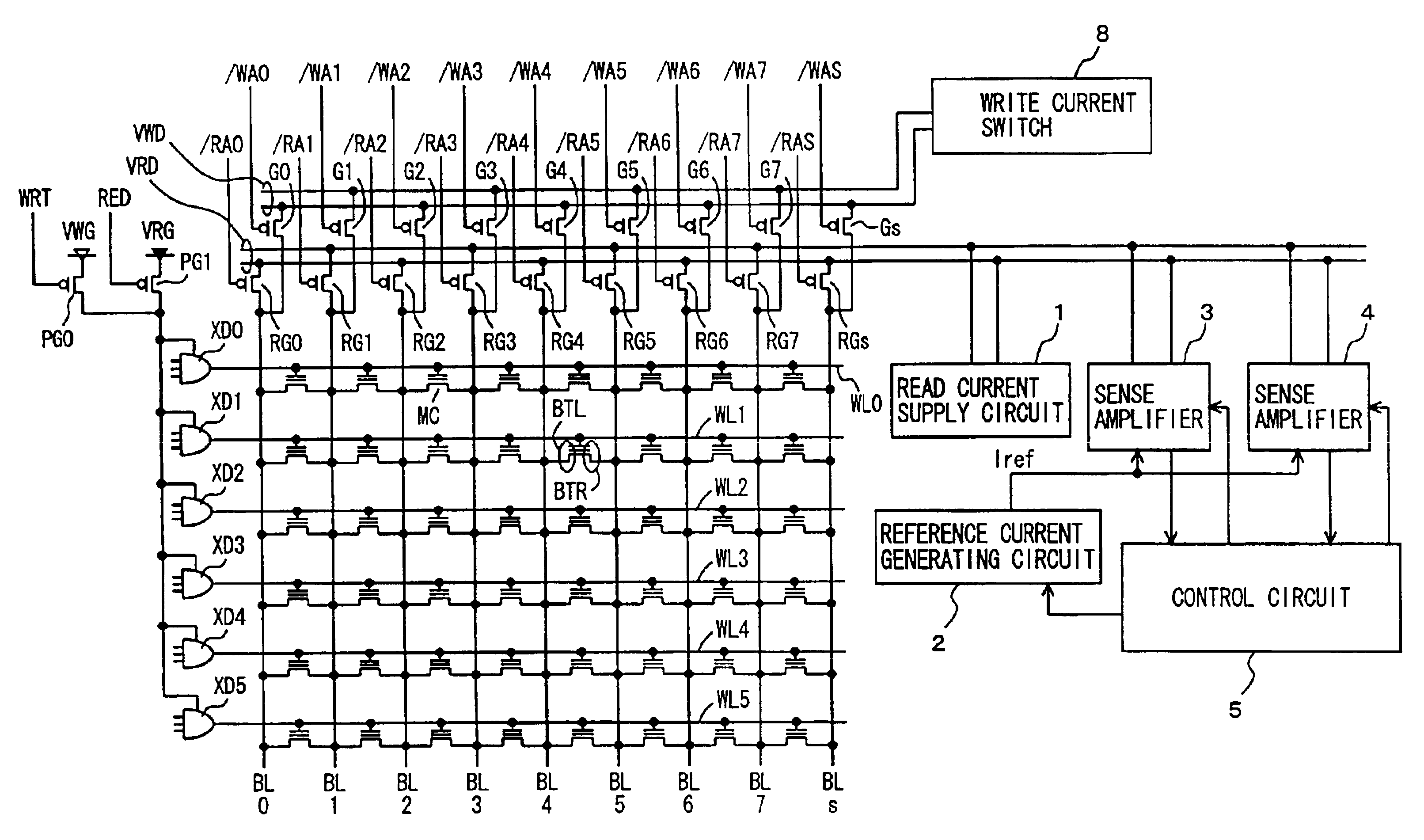
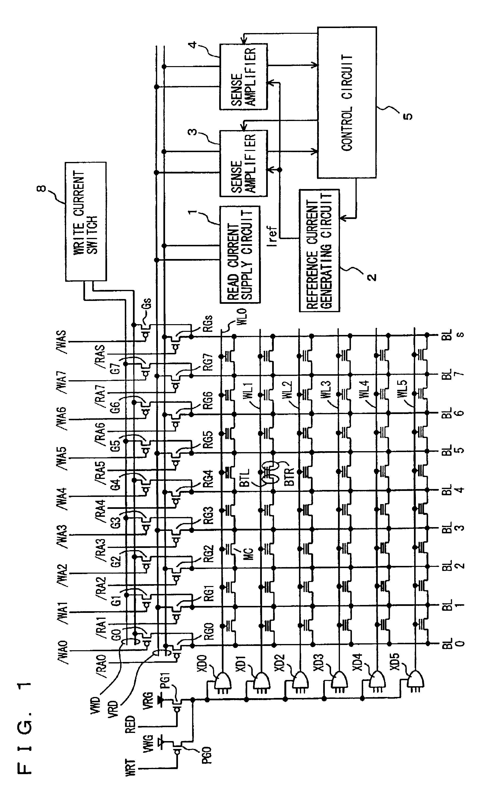
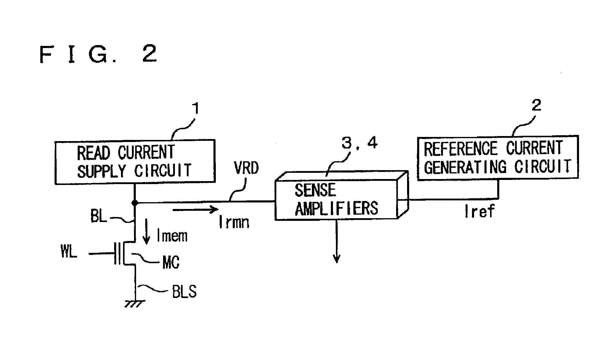
A configuration in which in data reading, set conditions for reading of data in a memory cell are changed according to the address of the memory cell can be applied to a general semiconductor memory device as well. That is, for example, in a case where a read voltage of a memory cell is low, when the memory cell of a low read voltage is selected, conditions set for reading from a memory cell are changed by adjusting an appropriate parameter among various parameters in the Thus, the read voltage from the memory cell can be equivalently increased to read memory cell data correctly.

While each embodiment is described with reference to an insulating film trapping type non-volatile semiconductor memory device storing data by accumulating electrons in an insulating film. As a non-volatile semiconductor memory device, however, a non-volatile semiconductor memory device storing data by accumulating electric charges in a floating gate formed of an electrically conductive material such as pol...

first embodiment

Furthermore, contrary to the first embodiment, written state and erased state of a memory cell may be correlated to a low threshold state and a high threshold state, respectively.

As described above, according to the present invention, detection is made on a sense margin failure due to a change in a threshold voltage characteristic of a memory cell and a parameter to determine a sense margin is changed so as to compensate for the margin failure. Accordingly, data in a memory cell with a margin failure can be read correctly without exerting an adverse influence on data reading from a normal memory cell.


PUM


Abstract

A plurality of sense amplifiers are connected to a selected bit line. Each sense amplifier is supplied with a residual current corresponding to a current flowing in a memory cell and a reference current serving as a reference for a threshold voltage of the memory cell to sense the currents. Operations of the sense amplifiers are controlled such that different sense margins are provided to different sense amplifiers and a margin failure is detected according to coincidence / non-coincidence in logical level between output signals of the sense amplifiers. The address of a memory cell with the margin failure is registered. With such a construction, a threshold voltage defect of a non-volatile memory cell is compensated for to enable internal reading of memory cell data with correctness.

Description

1. Field of the InventionThe present invention relates to a semiconductor memory device, and particularly, to a configuration of a data reading section in a non-volatile semiconductor memory device storing information in a non-volatile manner. More particularly, the present invention relates to a semiconductor memory device capable of correctly reading data even when a characteristic of a memory cell is deteriorated.2. Description of the Background ArtA non-volatile semiconductor memory device storing data in a non-volatile manner has been known as one of semiconductor memory devices. A memory cell of the non-volatile semiconductor memory device is constituted of one transistor. Data is stored by accumulating electric charges in a charge accumulating region electrically isolated from the surroundings of the memory cell transistor to change a threshold voltage of the memory cell transistor. Since electric charges (referred to as charges simply hereinafter) are stored in a charge accu...

Claims


Application Information

Patent Timeline
Patent Type & Authority Patents(United States)
IPC IPC(8): G11C16/34G11C16/28G11C16/06G11C16/02G11C16/04
CPCG11C16/3436G11C16/28
Inventor OOISHI, TSUKASAOHTANI, JUNKATO, HIROSHI
Owner RENESAS ELECTRONICS CORP
Why Eureka
Try Eureka