

Pixel driving circuit, driving method thereof, and display device
A pixel driving circuit, driving transistor technology, applied in circuits, electrical components, static indicators, etc., can solve problems such as inconsistency, uneven brightness of OLED display screens, and small size
- Summary
- Abstract
- Description
- Claims
- Application Information
AI Technical Summary
Problems solved by technology
Method used
Image

Examples
Embodiment 1
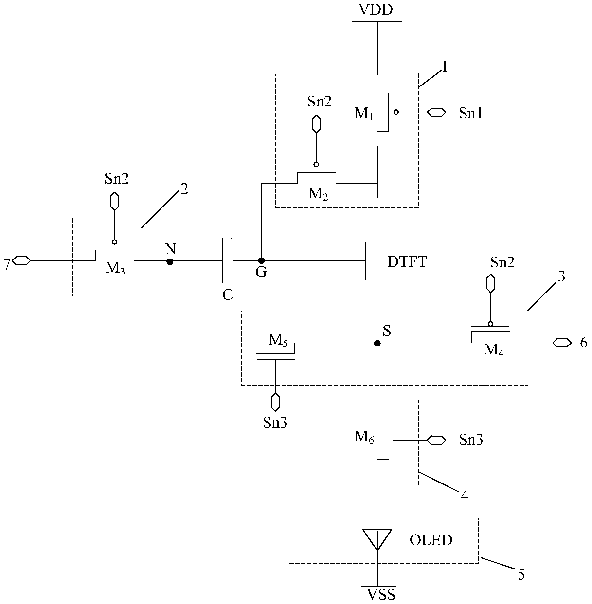
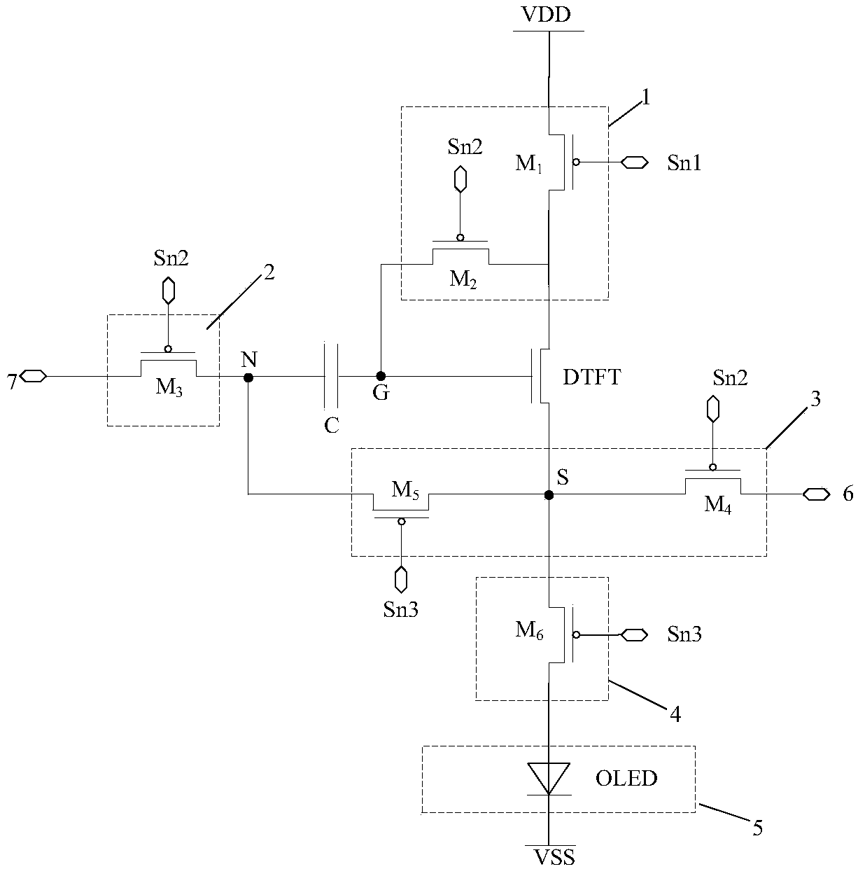
[0042] see figure 1 The pixel drive circuit provided in this embodiment includes a jump capacitor C, a reset unit 1, a data writing unit 2, a compensation unit 3, a light emission control unit 4, and a driving transistor DTFT for driving the light emitting unit 5 to emit light;
[0043] The output end of the reset unit 1 is connected to the first plate of the jump capacitor C, the output end of the data writing unit 2 is connected to the second plate of the jump capacitor C, and the output end of the compensation unit 3 is connected to the second plate of the jump capacitor C. The second plate is connected;
[0044] The first plate of the jump capacitor C is connected to the control terminal of the drive transistor DTFT, the output terminal of the reset unit 1 is also connected to the input terminal of the drive transistor DTFT, and the output terminal of the compensation unit 3 is also connected to the output terminal of the drive transistor DTFT and the output terminal of th...
Embodiment 2
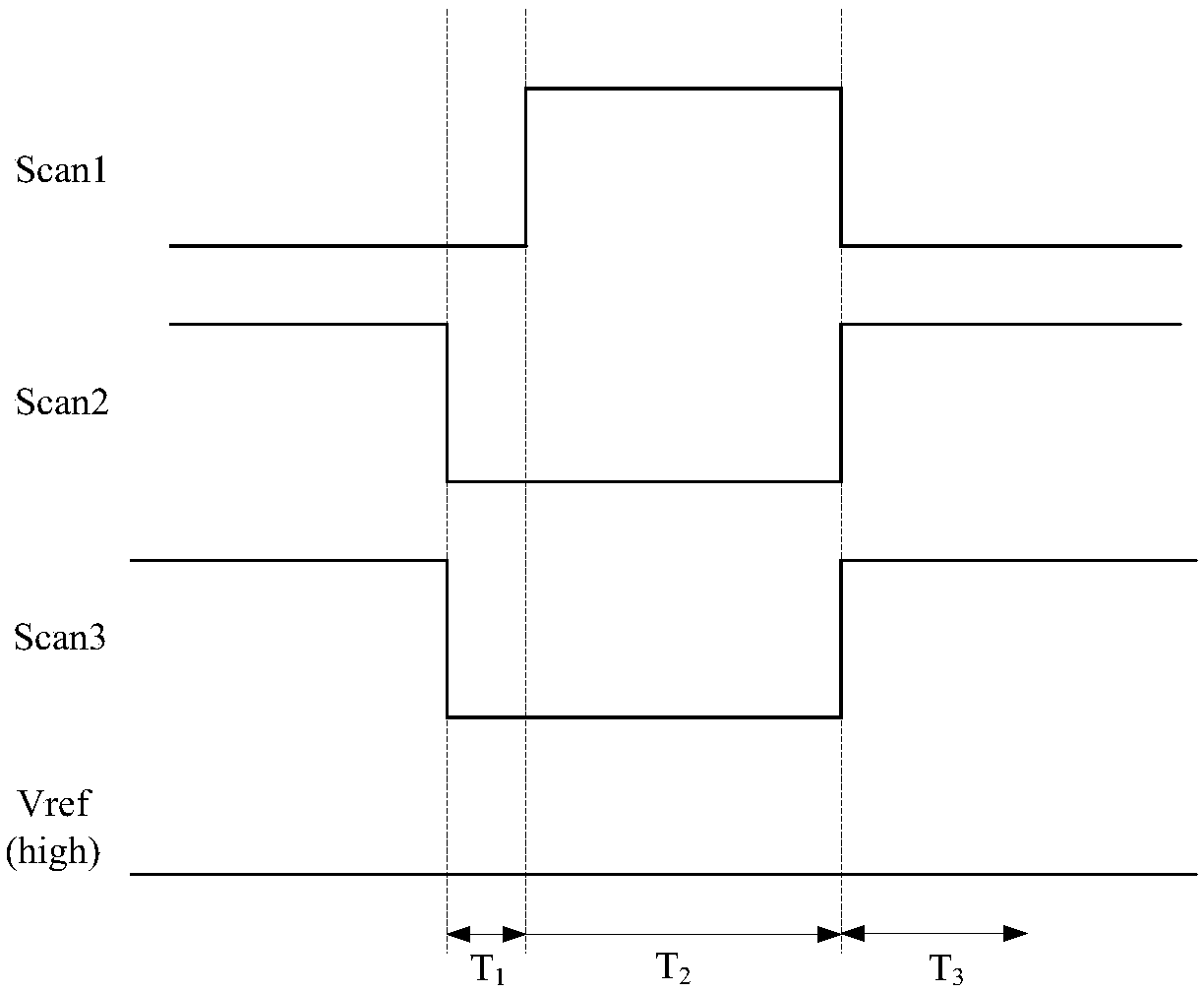
[0085] This embodiment also provides a driving method for a pixel driving circuit, which is applied to the pixel driving circuit in Embodiment 1; the driving method includes multiple driving cycles, and each driving cycle includes:
[0086] The first stage T 1 , the reset unit 1 clears the terminal voltage of the first plate of the jump capacitor C in the third stage of the last drive cycle, and controls the drive transistor DTFT to be turned on; the data writing unit 2 writes the data signal into the jump capacitor C second plate;
[0087] The second stage T 2 , the compensation unit 3 discharges the first plate of the jump capacitor C when the drive transistor DTFT is turned on until the drive transistor DTFT is turned off;
[0088] The third stage T 3 , the light emission control unit 4 reduces the output terminal voltage of the driving transistor DTFT, so that the driving transistor DTFT is turned on, and the light emitting unit 5 emits light; the compensation unit 3 tr...
Embodiment 3
[0103] This embodiment also provides a display device, which includes the pixel driving circuit as described in Embodiment 1. The display device can well avoid the problem of resistance voltage drop caused by too long power supply wires, so that the data signal The normal output ensures uniform brightness of the display screen.
[0104] It should be noted that the display device provided in the above embodiments may be any product or component with a display function, such as a mobile phone, a tablet computer, a television, a monitor, a notebook computer, a digital photo frame, or a navigator.
[0105] In the description of the above embodiments, specific features, structures, materials or characteristics may be combined in any one or more embodiments or examples in an appropriate manner.
PUM
 Abstract
Description
Claims
Application Information